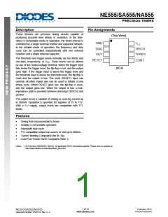
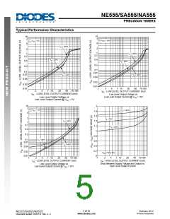
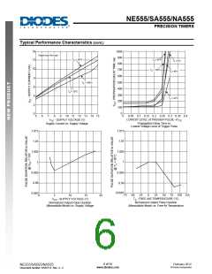
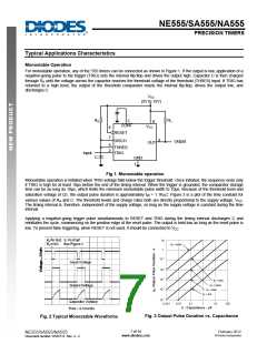
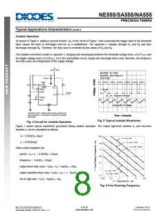
NE555/SA555/NA555
PRECISION TIMERS
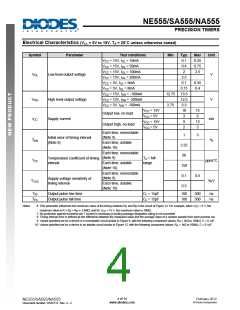
Electrical Characteristics (VCC = 5V to 15V, TA = 25°C unless otherwise stated)
Symbol
Parameter
Test conditions
CC = 15V, IOL = 10mA
Min
Typ.
0.1
0.4
2
Max
0.25
0.75
2.5
Unit
V
VCC = 15V, IOL = 50mA
VCC = 15V, IOL = 100mA
VCC = 15V, IOL = 200mA
VCC = 5V, IOL = 5mA
VOL
Low level output voltage
V
2.5
0.1
0.15
13.3
12.5
3.3
10
0.35
0.4
VCC = 5V, IOL = 8mA
VCC = 15V, IOH = -100mA
VCC = 15V, IOH = -200mA
VCC = 5V, IOH = -100mA
12.75
2.75
VOH
High level output voltage
Supply current
V
V
CC = 15V
15
6
Output low, no load
Output high, no load
VCC = 5V
VCC = 15V
VCC = 5V
3
ICC
mA
9
13
5
2
Each time, monostable
(Note 9)
1
3
Initial error of timing interval
(Note 8)
TER
%
Each time, astable
(Note 10)
2.25
50
Each time, monostable
(Note 9)
Temperature coefficient of timing
interval
TA = full
range
TTC
ppm/°C
%/V
Each time, astable
(Note 10)
150
0.1
0.3
Each time, monostable
(Note 9)
0.5
Supply voltage sensitivity of
timing interval
TVCC
Each time, astable
(Note 10)
TRI
Output pulse rise time
Output pulse fall time
CL = 15pF
CL = 15pF
100
100
300
300
ns
ns
TFA
Notes:
6. This parameter influences the maximum value of the timing resistors R and R in the circuit of Figure 12. For example, when V
= 5 V, the
CC
A
B
maximum value is R = R + R ≉ 3.4MΩ, and for V = 15 V, the maximum value is 10MΩ.
A
B
CC
7. No protection against excessive pin 7 current is necessary providing package dissipation rating is not exceeded
8. Timing interval error is defined as the difference between the measured value and the average value of a random sample from each process run.
9. Values specified are for a device in a monostable circuit similar to Figure 9, with the following component values: R = 2kΩ to 100kΩ, C = 0.1uF.
A
10. Values specified are for a device in an astable circuit similar to Figure 12, with the following component values: R = 1kΩ to 100kΩ, C = 0.1uF.
A
4 of 14
www.diodes.com
February 2012
© Diodes Incorporated
NE555/SA555/NA555
Document number: DS35112 Rev. 4 - 2
.图片预览")
 ETC [ ETC ]