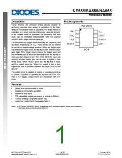
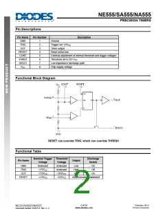
NE555/SA555/NA555
PRECISION TIMERS
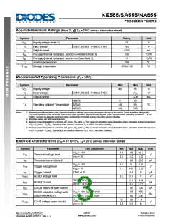
Absolute Maximum Ratings (Note 2) @ TA = 25°C unless otherwise stated
Symbol
VCC
VI
Parameter
Rating
18
Unit
V
Supply voltage (Note 3)
Input voltage
CONT, RESET, THRES, TRIG
VCC
V
IO
Output current
±225
130
mA
°C/W
°C/W
°C
θJA
Package thermal resistance Junction-to-Ambient (Note 4)
Package thermal resistance Junction-to-Case (Note 5)
Junction temperature
θJC
15
TJ
150
TSTG
Storage temperature
-65 to 150
°C
Recommended Operating Conditions (TA = 25°C)
Symbol
VCC
VI
Parameter
CONT, RESET, THRES, TRIG
NE555
Min
Max
16
Unit
V
Supply voltage
Input voltage
Output current
4.5
V
VCC
±200
70
IO
mA
0
TA
Operating Ambient Temperature SA555
NA555
-40
-40
85
°C
105
Notes:
2. Stresses beyond those listed under "absolute maximum ratings" may cause permanent damage to the device. These are stress ratings only.
Functional operation of the device at these or any other conditions beyond those indicated under "recommended operating conditions" is not
implied. Exposure to absolute-maximum-rated conditions for extended periods may affect device reliability.
3. All voltage values are with respect ground.
4. Maximum power dissipation is a function of T (max), θ , and T . The maximum allowable power dissipation at any allowable ambient temperature
J
JA
A
is P = (T (max) – T )/θ . Operating at the absolute maximum T of 150°C can affect reliability.
D
J
A
JA
J
5. Maximum power dissipation is a function of T (max), θ , and T . The maximum allowable power dissipation at any allowable ambient temperature
J
JC
A
is P = (T (max) – T )/θ . Operating at the absolute maximum T of 150°C can affect reliability.
D
J
C
JA
J
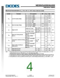
Electrical Characteristics (VCC = 5V to 15V, TA = 25°C unless otherwise stated)
Symbol
VTH
Parameter
Threshold voltage level
Threshold current (Note 6)
Trigger voltage level
Test conditions
Min
8.8
2.4
Typ.
10
Max
11.2
4.2
250
5.6
2.2
2
Unit
V
V
CC = 15V
VCC = 5V
3.3
30
ITH
nA
V
VCC = 15V
VCC = 5V
4.5
1.1
5
VTR
1.67
0.5
0.7
0.1
-0.4
20
ITR
Trigger current
TRIG at 0V
µA
V
VRST
RESET voltage level
0.3
1
RESET at VCC
RESET at 0V
0.4
-1.5
100
480
200
11
IRST
IDIS
RESET current
mA
nA
DISCH switch off-state current
VCC = 15V, IDIS = 15mA
VCC = 5V, IDIS = 4.5mA
180
80
DISCH saturation voltage with
output low (Note 7)
VDIS
mV
VCC = 15V
9
10
VCON
CONT voltage (open circuit)
V
VCC = 5V
2.6
3.3
4
3 of 14
www.diodes.com
February 2012
© Diodes Incorporated
NE555/SA555/NA555
Document number: DS35112 Rev. 4 - 2
.图片预览")
 ETC [ ETC ]