ICL7104
Pin Descriptions (Continued)
PIN NO.
21
SYMBOL
BIT 1
OPTION
DESCRIPTION
Least Significant Bit (LSB).
22
LBEN
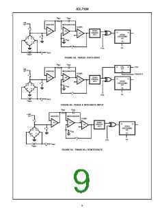
LOW BYTE ENABLE: If not in handshake mode (see pin 27) when LO (with CE/LD, pin 30)
activates low-order byte outputs, BITS 1-8. When in handshake mode (see pin 27), serves as a
low byte flag output. See Figures 11, 12, 13.
23
24
MBEN
HBEN
-16
-14
-16
-14
MID BYTE ENABLE: Activates Bits 9-16, see LBEN (pin 22)
HIGH BYTE ENABLE: Activates Bits 9-14, POL, OR, see LBEN (pin 22)
HIGH BYTE ENABLE: Activates POL, OR, see LBEN (pin 22).
RC oscillator pin: Can be used as clock output.
HBEN
CLOCK3
CLOCK 1
CLOCK 2
MODE
25
26
27
Clock Input: External clock or ocsillator.
Clock Output: Crystal or RC oscillator.
INPUT LO: Direct output mode where CE/LD, HBEN, MBEN and LBEN act as inputs directly
controlling byte outputs. If pulsed HI causes immediate entry into handshake mode (see Figure
13). If HI, enables CE/LD, HBEN, MBEN and LBEN as outputs. Handshake mode will be entered
and data output as in Figures 11 and 12 at conversion completion.
17
15
28
R/H
RUN/HOLD: Input HI conversions continuously performed every 2 (-16) or 2 (-14) clock
pulses. Input LO conversion in progress completed, converter will stop in Auto-Zero 7 counts
before input integrate.
29
30
SEN
SEND ENABLE: Input controls timing of byte transmission in handshake mode. HI indicates
‘send’.
CE/LD
CHIP ENABLE/ LOAD: WITH MODE (PIN 27) LO, CE/LD serves as a master output enable;
when HI, the bit outputs and POL, OR are disabled. With MODE HI, pin serves as a LOAD strobe
(-ve going) used in handshake mode. See Figures 11 and 12.
31
32
33
34
35
36
37
38
39
40
V+
Positive Logic Supply Voltage: Nominally +5V.
Analog Input: High Side.
AN I/P
BUF IN
REFCAP2
AN. GND
A-Z
Buffer Input: Buffer Analog to analog chip (ICL8052 or ICL8086).
Reference Capacitor: Negative Side.
Analog Ground: Input low side and reference low side.
Auto-Zero node.
V
Voltage Reference: Input (positive side).
Reference Capacitor: Positive side.
REF
REFCAP1
COMP-IN
V-
Comparator Input: From 8052/8068.
Negative Supply Voltage: Nominally -15V.
3

 ETC [ ETC ]