NCP1200
APPLICATIONS INFORMATION
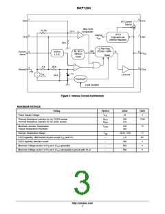
INTRODUCTION
Dynamic Self–Supply
The NCP1200 implements a standard current mode
architecture where the switch–off time is dictated by the
peak current setpoint. This component represents the ideal
candidate where low part–count is the key parameter,
particularly in low–cost AC/DC adapters, auxiliary supplies
etc. Thanks to its high–performance High–Voltage
technology, the NCP1200 incorporates all the necessary
components normally needed in UC384X based supplies:
timing components, feedback devices, low–pass filter and
self–supply. This later point emphasizes the fact that ON
Semiconductor’s NCP1200 does NOT need an auxiliary
winding to operate: the product is naturally supplied from
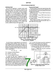
The DSS principle is based on the charge/discharge of the
V
bulk capacitor from a low level up to a higher level. We
CC
can easily describe the current source operation with a bunch
of simple logical equations:
POWER–ON: IF V < V
THEN Current Source
CC
CCOFF
is ON, no output pulses
IF V decreasing > V
OFF, output is pulsing
THEN Current Source is
THEN Current Source is
CC
CCON
IF V increasing < V
CC
CCOFF
ON, output is pulsing
Typical values are: V
= 11.4 V, V
= 9.8 V
CCOFF
CCON
To better understand the operational principle, Figure 15’s
sketch offers the necessary light:
the high–voltage rail and delivers a V to the IC. This
CC
system is called the Dynamic Self–Supply (DSS).
V
= 11.4 V
CCOFF
V
CC
10.6 V Avg.
V
CCON
= 9.8 V
ON
OFF
Current
Source
Output Pulses
50.00M 70.00M
10.00M
30.00M
90.00M
Figure 15. The Charge/Discharge Cycle
Over a 10 mF VCC Capacitor
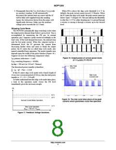
The DSS behavior actually depends on the internal IC
consumption and the MOSFET’s gate charge, Qg. If we
select a MOSFET like the MTD1N60E, Qg equals 11 nC
(max). With a maximum switching frequency of 48 kHz (for
the P40 version), the average power necessary to drive the
MOSFET (excluding the driver efficiency and neglecting
various voltage drops) is:
. 0.16 = 256 mW. If for design reasons this contribution is
still too high, several solutions exist to diminish it:
1. Use a MOSFET with lower gate charge Qg
2. Connect pin through a diode (1N4007 typically) to
one of the mains input. The average value on pin 8
2 * V
mains PEAK
becomes
. Our power contribution
p
example drops to: 160 mW.
Fsw @ Qg @ V
with
cc
Fsw = maximum switching frequency
Qg = MOSFET’s gate charge
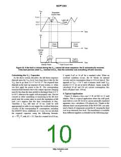
Dstart
1N4007
V
CC
= V level applied to the gate
GS
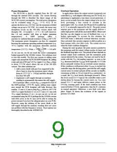
To obtain the final driver contribution to the IC
C3
4.7 mF
400 V
+
NCP1200
consumption, simply divide this result by V : Idriver =
CC
HV
NC
1
2
3
4
8
7
6
5
Fsw @ Qg = 530 µA. The total standby power consumption
at no–load will therefore heavily rely on the internal IC
consumption plus the above driving current (altered by the
driver’s efficiency). Suppose that the IC is supplied from a
400 V DC line. To fully supply the integrated circuit, let’s
imagine the 4 mA source is ON during 8 ms and OFF during
50 ms. The IC power contribution is therefore: 400 V . 4 mA
Adj
FB
CS
V
CC
EMI
Filter
Gnd Drv
Figure 16. A simple diode naturally reduces the
average voltage on pin 8
http://onsemi.com
7

 ETC [ ETC ]