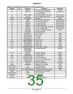
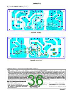
AND8327/D
L1
(eq. 5)
(eq. 6)
Re(VFB) + A1 cos ö1 ) A2 cos ö2 + X
Im(VFB) + A1 sinö1 ) A2 sin ö2 + Y
Vout
Vsweep
AC = 1 V
Vext
5 V
The rotating vector obtained at the end will be of the
following form:
+
+
Rled
1 k
R2
10 k
(eq. 7)
VFB + X ) jꢁY
B
A
Where we can now extract a module and an argument:
Fast
Lane
Slow
Lane
Ǹ
ø VFB ø+ Y2 ) X2
(eq. 8)
+
C1
100 nF
Cout
220 mF
Y
X
arg VFB + tan*1
ǒ Ǔ
Plotting 20log of Equation 8 and the phase returned by
(eq. 9)
U2B
10
Equationꢀ9 should give the Bode plot we are looking for.
U1
TL431
R3
10 k
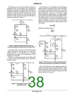
SPICE Application
Before rushing to the laboratory to apply this technique,
let's give it a try with a SPICE simulation and check that our
equations give the correct answers. Figure 6 depicts the
TL431 circuit ready to be ac swept, both inputs being
connected together. The sweep technique uses an old trick
Figure 5. The Fast Lane is Now ac Swept as the
Slow Lane is Simply dc Biased
with L and C which open the loop in ac but keep it closed
1
3
in dc. The closed path in dc helps to automatically adjust the
The dc adjustment might be a little difficult given the
open-loop gain brought by the TL431 and the sensitivity on
the external bias. The network analyzer still computes
voltage on the upper terminal of R to obtain a 2.5 V on the
2
feedback output, right in the middle of the available
dynamic. This ensures a circuit properly biased without the
need to tweak anything else. The bias points appearing in
Figureꢀ6 confirms the right values. Once the ac sweep is run
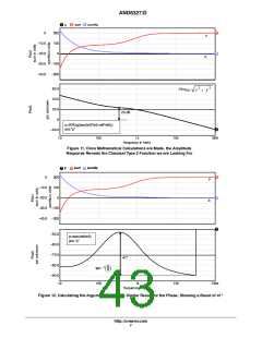
the Bode diagram appears in Figure 7 and confirms the
presence of an origin pole, a low frequency zero, a high
frequency pole and a mid-band gain in between. The phase
boost peaks to 134° at a frequency of 380 Hz where the gain
reaches 23ꢀdB. Now, let us separate the two lanes by
applying the technique we described earlier. The exploration
of the fast lane requires a simple dc bias on the divider
network, again provided by the operational amplifier.
Figureꢀ8 portrays the circuit we have implemented. The
modulation signal enters the fast lane through the ac source
20log (B/A) for the fast lane but this time, it plots a loop
10
gain equal to G (s).
1
Combining Signals Together
Once we have both slow and fast lanes loop plots on the
screen, how can we combine them? Can we just sum up the
gain and phase diagrams, respectively expressed in dB and
degrees? Certainly not, it would correspond to cascaded gain
blocks and not paralleled paths. We need to vector sum both
output signals and reconstruct the final signal which
expresses the combination of both loops. Using Euler
notation, we can express the slow lane signal by a rotating
vector affected by a module A and a phase ϕ :
1
1
Vout,slow + A1(cosö1 ) j sin ö1)
(eq. 3)
V
sweep
whereas L and C prevent any injection in the slow
1 4
lane: both loops are fully decoupled from each others. For
the slow lane sweep, Figure 9 shows the adopted sketch: the
upper LED resistor is simply hooked to a dc source and the
ac stimulus now sweeps the slow lane through the LC
network. Again, there is no ac link between both inputs.
Using a similar notation, we can write the fast lane
expression:
(eq. 4)
Vout,fast + A2(cosö2 ) j sinö2)
To reconstruct and plot the final gain curve combining
both signals − the signal observed on the feedback pin once
all loops are closed − we need to separate the real and
imaginary portions of the two lanes and sum them together:
http://onsemi.com
3

 ETC [ ETC ]