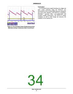
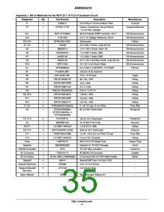
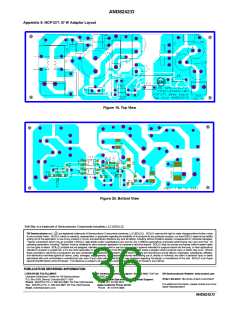
AND8327/D
The loop gain of such a system could be measured by
In this schematic, it is not possible to sweep both inputs
together as they are separated by the LC filter. Fortunately,
we can apply the superposition theorem as we are dealing
with a linear system. At first, we will sweep the slow lane
while keeping the fast lane to a bias level, totally
disconnected from the output voltage. A dc voltage supplied
by an external source will do. This is what Figure 4 shows.
The precision of the 5 V source is not relevant here as it only
serves bias purposes. The ac source actually represents an
injection transformer, classically used in loop stability
studies. The A and B probes go to a network analyzer which
will compute
breaking the loop at the feedback point. Unfortunately,
depending on the converter configuration, this solution can
sometimes be difficult to implement. The best is then to
measure the loop gain from the secondary side. In this
particular example, both the fast and slow lanes share a
similar entry point. The total loop gain could therefore be
measured as suggested by Figure 2:
Vout
V1
AC = 1
+
B
A
ǒ Ǔꢀ,
20log10
Rled
1 k
R2
10 k
displaying a loop gain equal to
Fast
Lane
Slow
Lane
G1(s)
sR2C1
C1
100 nF
U2B
L1
Vout
U1
TL431
Vsweep
AC = 1 V
+
R3
10 k
+
Rled
Vext
1 k
5 V
R2
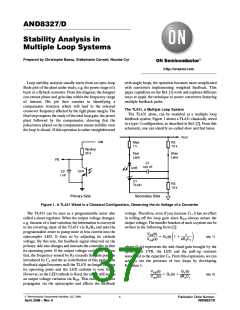
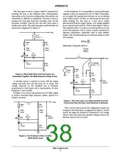
Figure 2. When Both Slow and Fast Lanes are
Connected Together, the Measurement is Easy to Run
Fast
Lane
10 k
B
A
Slow
Lane
+
C1
100 nF
Cout
220 mF
A stimulus source is inserted in series with the output
voltage and both slow and fast lanes are ac swept. The
voltage observed on the feedback pin is therefore
proportional to both inputs and is representative of what
Equationsꢀ1 and 2 predict.
In Figure 3, we can see the presence of a LC filter, added
to remove unwanted high frequency spikes, typical of a
flyback converter.
U2B
U1
TL431
R3
10 k
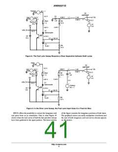
Figure 4. The Fast Lane is ac Disconnected from the
Circuit and Only the Slow Lane Receives a Stimulus
Vout
L1
Rled
1 k
R2
10 k
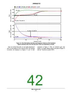
Then, once the plot is saved, the configuration needs to be
changed to the other input, as suggested by Figure 5. In this
circuit, the upper R terminal is connected to a dc voltage
Fast
Lane
Slow
Lane
2
+
whose value must equal the regulated voltage whereas the
fast lane input is now ac swept:
C1
100 nF
Cout
220 mF
U2B
U1
TL431
R3
10 k
Figure 3. The Presence of the LC Filter
Splits Both Lanes
http://onsemi.com
2

 ETC [ ETC ]