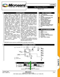
LX1992
High Efficiency LED Driver
L I N F I N I T Y D I V I S I O N
PRODUCTION
APPLICATION INFORMATION
OPERATING THEORY
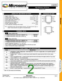
INDUCTOR SELECTION AND OUTPUT CURRENT LIMIT
PROGRAMMING
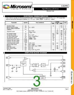
The LX1992 is a PFM boost converter that is
optimized for driving a string of series connected LEDs. It
operates in a pseudo-hysteretic mode with a fixed switch
“off time” of 300ns. Converter switching is enabled as
LED current decreases causing the voltage across RSET to
decrease to a value less than the voltage at the VADJ pin.
When the voltage across RSET (i.e., VFB) is less than VADJ,
comparator A activates the control logic. The control logic
activates the DRV output circuit that connects to the gate
of the external FET. The DRV output is switched “on”
(and remains “on”) until the inductor current ramps up to
the peak current level. This current level is set via the
external RCS resistor and monitored through the CS and
SRC inputs by comparator B.
Setting the level of peak inductor current to approximately
2X the expected maximum DC input current will minimize
the inductor size, the input ripple current, and the output
ripple voltage. The designer is encouraged to use inductors
that will not saturate at the peak inductor current level. An
inductor value of 47µH is recommended. Choosing a lower
value emphasizes peak current overshoot while choosing a
higher value emphasizes output ripple voltage. The peak
switch current is defined using a resistor placed between the
CS terminal and ground and the IPEAK equation is:
V
I
CS
+
t +
R
IN
IPEAK = IMIN
D
CS
L
R
ICS
The LED load is powered from energy stored in the
output capacitor during the inductor charging cycle. Once
the peak inductor current value is achieved, the NDRV
output is turned off (off-time is typically 300ns) allowing a
portion of the energy stored in the inductor to be delivered
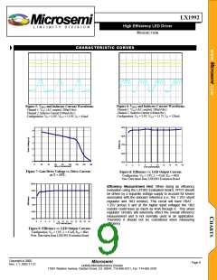
to the load (e.g., see Figure 5, channel 2). This causes the
output voltage to continue to rise across RSET at the input to
the feedback circuit. The LX1992 continues to switch until
the voltage at the FB pin exceeds the control voltage at the
ADJ pin.
The maximum IPEAK value is limited by the ISRC value
(max. = 0.8ARMS). The minimum IPEAK value is defined
when RCS is zero. The value range for parameters IMIN and
ICS
section of this data sheet. The parameter tD
are provided in the ELECTRICAL CHARiAsCrTeElRatIeSdTICtoS
internal operation of the device. A typical value at 25oC is
800ns. RICS is the internal current sense resistor connected to
the SRC pin. A typical value at 25oC is 200mΩ. All of these
parameters have an effect on the final IPEAK value.
DESIGN EXAMPLE:
Determine IPEAK where VIN equals 3.0V and RCS equals
4.02KΩ using nominal values for all other parameters.
The value of RSET is established by dividing the
maximum adjust voltage by the maximum series LED
current. A minimum value of 15Ω is recommended for
R
SET. The voltage at the FB pin is the product of IOUT (i.e.,
5.0µA
3.0V
IPEAK = 73mA+
×800ns+
×4.02KΩ
the current through the LED chain) and RSET
V
.
47µH
200mΩ
The result of this example yields a nominal IPEAK of
approximately 225mA.
ADJmaxI
RSET
=
LEDmax
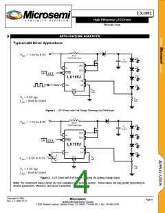
The application of an external voltage source at the
ADJ pin provides for output current adjustment over the
entire dimming range and the designer can select one of
two possible methods. The first option is to connect a
PWM logic signal to the ADJ pin (e.g., see Figure 1). The
LX1992 includes an internal 50pF capacitor to ground that
works with an external resistor to create a low-pass filter
(i.e., filter out the AC component of a pulse width
modulated input of fPWM ≥ 100KHz). The second option is
to adjust the reference voltage directly at the ADJ pin by
applying a DC voltage from 0.0 to 0.3V (e.g., see Figure
2). The adjustment voltage level is selectable (with limited
accuracy) by implementing the voltage divider created
between the external series resistor and the internal 2.5MΩ
resistor. Disabling the LX1992 is achieved by driving the
SHDN pin with a low-level logic signal thus reducing the
device power consumption to less than 0.5µA (typ).
OUTPUT RIPPLE AND CAPACITOR SELECTION
Output voltage ripple is a function of the inductor value
(L), the output capacitor value (COUT), the peak switch
current setting (IPEAK), the load current (IOUT), the input
voltage (VIN) and the output voltage (VOUT) for a this boost
converter regulation scheme. When the switch is first turned
on, the peak-to-peak voltage ripple is a function of the
output droop (as the inductor current charges to IPEAK), the
feedback transition error (i.e., typically 10mV), and the
output overshoot (when the stored energy in the inductor is
delivered to the load at the end of the charging cycle).
Therefore the total ripple voltage is
V
RIPPLE = ∆VDROOP + ∆VOVERSHOOT + 10mV
The initial droop can be estimated as follows where the
0.5 value in the denominator is an estimate of the voltage
drop across the inductor and the FET’s RDS_ON: The
Copyright 2000
Rev. 1.1, 2002-11-21
Microsemi
Page 5
Linfinity Microelectronics Division
11861 Western Avenue, Garden Grove, CA. 92841, 714-898-8121, Fax: 714-893-2570

 ETC [ ETC ]