LX1992
High Efficiency LED Driver
L I N F I N I T Y D I V I S I O N
PRODUCTION
ABSOLUTE MAXIMUM RATINGS
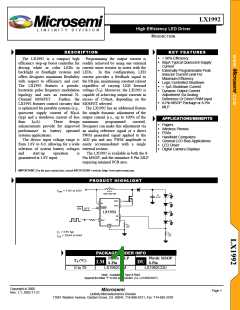
PACKAGE PIN OUT
Supply Voltage (VIN) ....................................................................... -0.3V to 7.0V
Feedback Input Voltage (VFB).................................................-0.3V to VIN + 0.3V
Shutdown Input Voltage (VSHDN) ...........................................-0.3V to VIN + 0.3V
Analog Adjust Input Voltage (VADJ).......................................-0.3V to VIN + 0.3V
Source Input Current (ISRC).................................................................... 0.80 ARMS
Operating Junction Temperature.................................................................. 150°C
Storage Temperature Range...........................................................-65°C to 150°C
Lead Temperature (Soldering 180 seconds)................................................. 235°C
1
2
3
4
8
7
6
5
SRC
GND
CS
DRV
IN
FB
SHDN
ADJ
DU PACKAGE
(Top View)
Note: Exceeding these ratings could cause damage to the device. All voltages are with respect to
Ground. Currents are positive into, negative out of specified terminal.
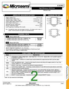
SRC
GND
CS
1
2
3
4
8
7
6
5
DRV
IN
FB
THERMAL DATA
ADJ
SHDN
LM PACKAGE
(Top View)
Plastic MSOP 8-Pin
DU
THERMAL RESISTANCE-JUNCTION TO AMBIENT, θJA
THERMAL RESISTANCE-JUNCTION TO CASE, θJC
206°C/W
39°C/W
Plastic MLP 8-Pin
LM
THERMAL RESISTANCE-JUNCTION TO AMBIENT, θJA
41°C/W
5.2°C/W
THERMAL RESISTANCE-JUNCTION TO CASE, θJC
Junction Temperature Calculation: T = T + (P x θ ).
JC
J
A
D
The θJA numbers are guidelines for the thermal performance of the device/pc-board
system. All of the above assume no ambient airflow.
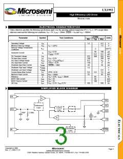
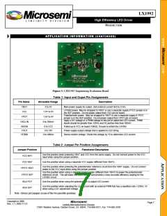
FUNCTIONAL PIN DESCRIPTION
NAME
DESCRIPTION
Unregulated IC Supply Voltage Input – Input range from +1.6V to 6.0V. Bypass with a 1µF or greater capacitor
IN
for operation below 2.0V.
Feedback Input – Connects to a current sense resistor between the output load and GND to set the output
FB
current.
Active-Low Shutdown Input – A logic low shuts down the device and reduces the supply current to 0.2µA (Typ).
SHDN
Connect
to VCC for normal operation.
SHDN
DRV
CS
GND
MOSFET Gate Driver – Connects to an external N-Channel MOSFET.
Current-Sense Amplifier Input – Connecting a resistor between CS and GND sets the peak inductor current limit.
Common terminal for ground reference.
Adjustment Signal Input – Provides the internal reference, via an internal filter and gain resistor, allowing a
dynamic output current adjustment corresponding to a varying duty cycle. The actual ADJ pin voltage range is
ADJ
from VIN to GND. In order to minimize the current sense resistor power dissipation a practical range of VADJ
0.0V to 0.5V should be used.
=
SRC
MOSFET Current Sense Input - Connects to the External N-Channel MOSFET Source.
Note: ADJ pin should not be left floating.
Copyright 2000
Rev. 1.1, 2002-11-21
Microsemi
Page 2
Linfinity Microelectronics Division
11861 Western Avenue, Garden Grove, CA. 92841, 714-898-8121, Fax: 714-893-2570

 ETC [ ETC ]