LHF80V25
31
sharp
(1)
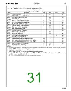
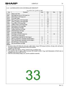
6.2.6 ALTERNATIVE CE#-CONTROLLED WRITES
V
=4.5V-5.5V, T =0°C to +70°C
A
CC
Sym.
Parameter
Notes
Min.
85
1
Max.
Unit
ns
µs
ns
ns
ns
ns
ns
ns
ns
ns
ns
ns
ns
ns
ns
ns
ns
ns
ns
ns
t
t
t
t
t
t
t
t
t
t
t
t
t
t
t
t
t
t
t
t
Write Cycle Time
AVAV
PHEL
WLEL
ELEH
PHHEH
SHEH
VPEH
AVEH
DVEH
EHDX
EHAX
EHWH
EHEL
EHRL
EHGL
QVVL
QVPH
QVSL
FVEH
EHFV
RP# High Recovery to CE# Going Low
WE# Setup to CE# Going Low
CE# Pulse Width
2
0
50
100
100
100
40
40
0
RP# V Setup to CE# Going High
2
2
2
3
3
HH
WP# V Setup to CE# Going High
IH
V
Setup to CE# Going High
PP
Address Setup to CE# Going High
Data Setup to CE# Going High
Data Hold from CE# High
Address Hold from CE# High
WE# Hold from CE# High
CE# Pulse Width High
5
0
25
CE# High to RY/BY# Going Low
Write Recovery before Read
90
0
0
V
Hold from Valid SRD, RY/BY# High Z
2,4
2,4
2,4
5
PP
RP# V Hold from Valid SRD, RY/BY# High Z
0
HH
WP# V Hold from Valid SRD, RY/BY# High Z
0
IH
BYTE# Setup to CE# Going High
BYTE# Hold from CE# High
40
85
5
NOTES:
1. In systems where CE# defines the write pulse width (within a longer WE# timing waveform), all setup, hold, and inactive
WE# times should be measured relative to the CE# waveform.
2. Sampled, not 100% tested.
3. Refer to Table 4 for valid A and D for block erase or word/byte write.
IN
IN
4. V should be held at V
(and if necessary RP# should be held at V ) until determination of block erase or
PP
PPH1/2
HH
word/byte write success (SR.1/3/4/5=0).
5. If BYTE# switch during reading cycle, exist the regulations separately.
Rev. 1.1

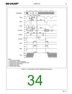
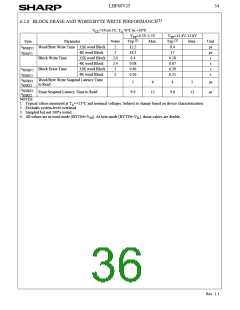
 ETC [ ETC ]
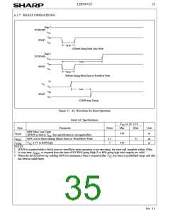