ICs for TV
AN5195K-C
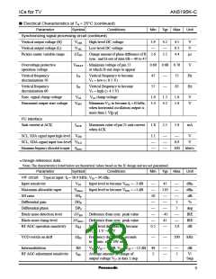
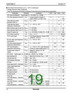
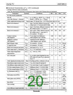
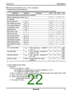
■ Electrical Characteristics at Ta = 25°C (continued)
Parameter
Symbol
Conditions
Min
Typ Max
Unit
Synchronizing signal processing circuit (continued)
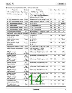
Vertical output voltage (H)
Vertical output voltage (L)
Picture center variable range
V58H
V58L
∆THC
High-level DC voltage
Low-level DC voltage
3.9
4.2
3.2
4.5
0.3
4.4
V
V
Change amount of phase difference of H 2.6
µs
sync. and H-out of data 0B = 40 to 47
Overvoltage protective
operation voltage
VXRAY Minimum voltage of pin 55
at which H-out stops to appear
0.60 0.68 0.76
V
Vertical frequency
discrimination 50
f50
Vertical frequency to become
V5 = low (< 0.5 V)
47
57
55
63
Hz
Hz
Vertical frequency
discrimination 60
f60
Vertical frequency to become
V5 = high (> 4.5 V)
Sync. signal clamp voltage
V46
V46 clamp voltage
1.0
1.3
4.2
1.6
5.0
V
V
Horizontal output start voltage
VfHS
Minimum V50 to become f0 >10 kHz, 3.4
when horizontal oscillation output is
more than 1 V[p-p]
I2C interface
Sink current at ACK
IACK
Maximum value of pin 21 sink current
when ACK
1.8
3.1
2.5
5.0
mA
SCL, SDA signal input high-level VIHI
SCL, SDA signal input low-level VILO
V
V
0.9
Maximum frequency allowable to input
fImax
100
kbit/s
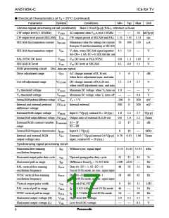
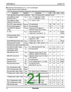
• Design reference data
Note) The characteristics listed below are theoretical values based on the IC design and are not guaranteed.
Parameter
Symbol
Conditions
Min
Typ Max
Unit
VIF circuit Typical input: fP = 38.9 MHz, VIN = 90 dBµ
Input sensitivity
VPS
VPmax
SNP
Input level to become VPO1 = −3 dB
Input level to become VPO1 = +1 dB
45
dBµ
dBµ
dB
Maximum allowable input
SN ratio
110
50
Differential gain
DGP
DPP
5
%
Differential phase
5
deg
IRE
IRE
dB
Black noise detection level
Black noise clamp level
RF AGC operation sensitivity
∆VBN
Deference from sync. peak value
−45
∆VBNC Deference from sync. peak value
45
GRF
Input level difference to become
0.5
3.0
V27 = 1 V → 7 V
VCO switch on drift
∆fPD
Frequency drift from 5 seconds
to 5 mins. after SW on
200
5
kHz
dB
Intermodulation
IM
VfC −VfP = −2 dB, VfC −VfP = −12 dB 46
RF AGC adjustment sensitivity
SRF
Average amount of change of
output voltage V27 at data 1 step
2
V/
Step
9

 ETC [ ETC ]