AN5195K-C
ICs for TV
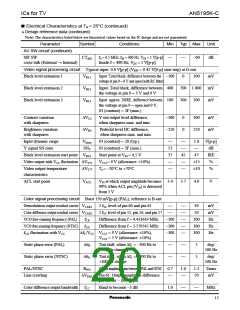
■ Electrical Characteristics at Ta = 25°C (continued)
• Design reference data (continued)
Note) The characteristics listed below are theoretical values based on the IC design and are not guaranteed.
Parameter
Symbol
Conditions
Min
Typ Max
Unit
Color signal processing circuit (continued) Burst 150 mV[p-p] (PAL), reference is B-out
Color-difference output
fluctuation with VCC
∆VC/V VCC1 = 9 V (allowance: ±10%),
VCC3 = 5 V (allowance: ±10%)
±15
±15
570
%
%
Color-difference output
temperature characteristics
∆VC/T
Ta= −20°C to +70°C
PAL/NTSC output impedance RO60,61PN DC measurement
390
100
−60
480
Ω
SECAM output impedance
RO60,61S DC measurement
kΩ
mV
Color/B&W DC difference
voltage
∆VCBW Pedestal level DC difference,
0
60
when burst signal with or without
(C−Y)/Y
RC/Y
Color bar input, B-out
Contrast typ., color data 00 = 30
0.9
1.2
1.5 V[0-p]/
V[0-p]
RGB processing circuit
YS changeover speed
fYS
fYS, when YS input is 3 V[0-p],
7
MHz
output level −3 dB
External RGB input dynamic range VDEXT
Internal/external crosstalk CTRGB
Synchronizing signal processing circuit
Contrast max., data 03 = 3F
1.0
V[p-p]
Leakage, when f = 1 MHz, 1 V[p-p], YS = 5 V
−50
dB
Lock detection output voltage
VLD
ILD
V18, when horizontal AFC lock
DC measurement
5.7
6.3
6.9
V
Lock detection charge
and discharge current
±0.6 ±0.8 ±1.1
mA
EBP (RGB) slice level
VFBP
Minimum voltage of pin 50, when
blanking is applied to RGB output
0.4
1.5
0.75
1.9
1.1
2.3
44
V
V
EBP (AFC2) slice level
VFBPH
Minimum voltage of pin 50 at which
AFC2 operates
Horizontal AFC µ
µH
βH
DC measurement
30
1.4
0.2
37
1.9
0.4
µA/µs
Horizontal VCO β
β curve gradient near f = 15.75 kHz
2.4 Hz/mV
Burst gate pulse position
PBGP
For both PAL/NTSC,
0.6
µs
delay from H. sync. rise
PAL burst gate pulse width
NTSC burst gate pulse width
Burst gate pulse output voltage
WBGPP
WBGPN
VBGP
3.4
2.5
4.5
4.0
3.0
4.7
2.4
4.6
3.5
4.9
2.7
µs
µs
V
DC voltage of pin 62 in BGP period
H blanking pulse output voltage VHBLK
DC voltage in H-blanking pulse period 2.1
of pin 62
V
V blanking pulse output voltage VVBLK
DC voltage in V-blanking pulse period 2.1
of pin 62
2.4
2.7
V
PAL V blanking pulse width
NTSC blanking pulse width
FBP allowable range
WVP
WVN
TFBP
Pulse width at f = 15.625 kHz
Pulse width at f = 15.75 kHz
Time from H-out rise to FBP center
1.31 1.41 1.51
1.01 1.11 1.21
ms
ms
µs
12
19
12

 ETC [ ETC ]