DC INPUTS
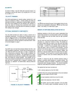
TABLE 6. PRECHARGE AMPLIFIER
GAIN PROGRAMMING
As noted in TABLE 1 the RD-19.30 will accept DC inputsꢀ It is
necessary to set the REF input to DC by tying RH to +5 V and
RL to GND or -5 \/ꢀ
UP/DN
GAIN
4
Logic 0
Logic 1
-5 V
1/4
1
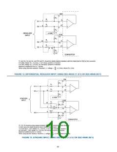
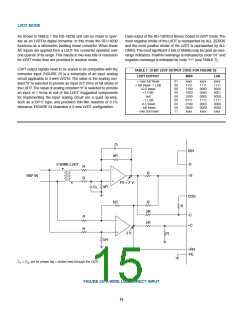
VELOCITY TRIMMING
RD-19.30 specifications for velocity scaling, reversal error, and
offset are contained in TABLE 1ꢀ Velocity scaling and offset are
externally trimmable for applications requiring tighter specifica-
tions than those available from the standard unitꢀ FIGURE 15
shows the setup for trimming these parameters with external
potsꢀ It should also be noted that when the resolution is changed,
VEL Scaling is also changedꢀ
UP/DN
The UP/DN input selects the gain of the amplifier driving the de-
selected set of bandwidth componentsꢀ UP/DN has three input
statesꢀ See TABLE 6 to relate input to gainꢀ
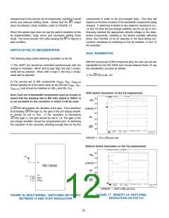
BENEFIT OF SWITCHING RESOLUTION ONTHE FLY
OPTIONAL BANDWIDTH COMPONENTS
Switching resolution on the fly can be used in applications that
require high resolution for accurate position control, and tracking
rates or settling times that are faster than the high resolution
mode will allowꢀ
The RD-19.30 provides the option of using a second set of
bandwidth componentsꢀ The second set of components can be
used for switch-on-the-fly or dual-bandwidth applicationsꢀ The
SHIFT and UP/DN inputs are used when when switching band-
width components, and their operation is described belowꢀ Refer
to the block diagram on page 1ꢀ
The RD-19.30 can track four times faster for each step down in
resolution (iꢀeꢀ, a step from 16 bits to 14 bits)ꢀ The velocity out-
put will be scaled down by a factor of four with each step down
in resolutionꢀ For example, if the velocity output is scaled such
that 4 Volts = 10 RPS in 16 bit resolution, then the same con-
verter will output 1 Volt for 10 RPS in 14 bit resolutionꢀ To avoid
glitches in the velocity output, the second set of bandwidth com-
ponents can be pre-charged to the expected voltage, and
switched in using the SHIFT input at the same time the resolu-
tion is changedꢀ This will allow for a smooth velocity transition,
resulting in reduced errors and minimal settling time after the
changeꢀ
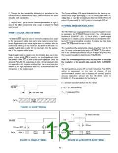
SHIFT
The SHIFT pin is an input that chooses between the VEL1 and
VEL. bandwidth componentsꢀ This pin has an internal pull-up to
+5Vꢀ When the SHIFT pin is left open, or a logic 1 is applied, the
VEL1 components are selectedꢀ When a Logic 0 is applied, the
VEL. components are selectedꢀ The deselected set of band-
width components are driven by an amplifier, with programmable
gain, that follows the velocity amplifierꢀ This amplifier can be
used to pre-charge the deselected set of components to the volt-
age level that is expected after a change in resolutionꢀ (See
description on BENEFIT OF SWITCHING RESOLUTION ON
THE FLYꢀ)
FIGURE 17 shows the way the converter behaves during a
change in resolution while tracking at a constant velocityꢀ The
first illustration shows the benefits of switching in pre-charged
components while changing resolutionꢀ The second illustration
shows the result without the benefits of switching on the flyꢀ
The signals that have been recorded are:
1) VEL: velocity output pin on the RD-19.30
+5 V
100 R
V
.
100 kΩ
-VCO
(OFFSET)
-5 V
0ꢀ8 R
V
.) ERROR: this is the analog representation of the error between
the input and the output of the RD-19.30
RD-19.30
0ꢀ4 R (SCALING)
V
3) D0: an input resolution control line to the RD-19.30
4) BIT: built-in-test output pin of the RD-19.30
1
VEL
When this system uses the switch resolution on the fly imple-
mentation, the velocity signal immediately assumes the pre-
FIGURE 15. VELOCITY TRIMMING
11

 ETC [ ETC ]