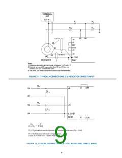
SIN
3
R
R
f
R
R
i
i
-S
1
6
-
S1
S3
.
5
+S
+
f
f
4
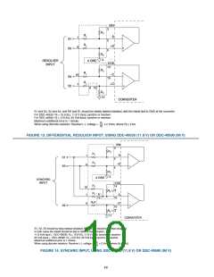
RESOLVER
INPUT
A GND
COS
13
R
R
R
i
i
-C
15
16
7
-
S4
S.
+C
+
8
10
R
f
1.
CONVERTER
S1 and S3, S. and S4, and RH and RL should be ideally twisted shielded, with the shield tied to GND at the converterꢀ
For DDC-49530: R = 70ꢀ8 KΩ, 11ꢀ8 V input, synchro or resolverꢀ
i
For DDC-49590: R = .70 KΩ, 90 Volt input, synchro or resolverꢀ
i
Maximum additional error is 1 minuteꢀ
When using discrete resistors: Resolver L-L voltage =
R
R
i
f
x . Vrms, where R ≥ 6 kΩ
f
FIGURE 13. DIFFERENTIAL RESOLVER INPUT, USING DDC-49530 (11.8 V) OR DDC-49590 (90 V)
SIN
3
R
f
R
i
-S
1
6
-
S1
S3
.
5
R
i
+S
+
R
f
4
A GND
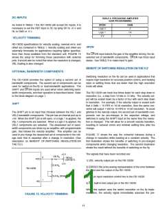
SYNCHRO
INPUT
COS
14
R
R
i
i
16
7
R /
f
3
8
15
-C
15
-
R /.
i
+C
10
9
+
S.
R /
f
3
11
CONVERTER
S1, S., S3 should be triple twisted shielded; RH and RL should be twisted shielded;
In both cases the shield should be tied to GND at the converterꢀ
11ꢀ8 Volt input = DDC-49530: R = 70ꢀ8 KΩ, 11ꢀ8 V input, synchro or resolverꢀ
i
90 Volt input = DDC-49590: R = .70 KΩ, 90 Volt input, synchro or resolverꢀ
i
Maximum additional error is 1 minuteꢀ
When using discrete resistors: Resolver L-L voltage =
R
R
i
f
x . Vrms, where R ≥ 6 kΩ
f
FIGURE 14. SYNCHRO INPUT, USING DDC-49530 (11.8 V) OR DDC-49590 (90 V)
10

 ETC [ ETC ]