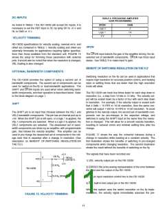
LVDT MODE
As shown in TABLE 1 the RD-19.30 unit can be made to oper-
ate as an LVDT-to-digital converterꢀ In this mode the RD-19.30
functions as a ratiometric tracking linear converterꢀ When linear
AC inputs are applied from a LVDT the converter operates over
one quarter of its rangeꢀThis results in two less bits of resolution
for LVDT mode than are provided in resolver modeꢀ
Data output of the RD-19.30 is Binary Coded in LVDT modeꢀThe
most negative stroke of the LVDT is represented by ALL ZEROS
and the most positive stroke of the LVDT is represented by ALL
ONESꢀThe most significant . bits (. MSBs) may be used as over-
range indicatorsꢀ Positive overrange is indicated by code “01” and
negative overrange is indicated by code “11“ (see TABLE 7)ꢀ
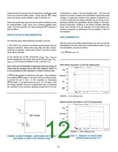
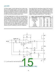
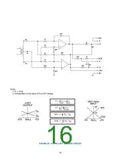
LDVT output signals need to be scaled to be compatible with the
converter inputꢀ FIGURE .5 is a schematic of an input scaling
circuit applicable to 3-wire LVDTsꢀ The value of the scaling con-
stant “a” is selected to provide an input of . Vrms at full stroke of
the LVDTꢀThe value of scaling constant “b” is selected to provide
an input of 1 Vrms at null of the LVDTꢀ Suggested components
for implementing the input scaling circuit are a quad op-amp,
such as a OP11 type, and precision thin-film resistors of 0ꢀ1%
toleranceꢀ FIGURE .4 illustrates a .-wire LVDT configurationꢀ
TABLE 7. 12-BIT LVDT OUTPUT CODE FOR FIGURE 25
LVDT OUTPUT
MSB
LSB
+ over full travel
+ full travel -1 LSB
+0ꢀ5 travel
+1 LSB
null
- 1 LSB
-0ꢀ5 travel
- full travel
- over full travel
01
00
00
00
00
00
00
00
11
xxxx
1111
1100
1000
1000
0111
0100
0000
xxxx
xxxx
1111
0000
0000
0000
1111
0000
0000
xxxx
xxxx
1111
0000
0001
0000
1111
0000
0000
xxxx
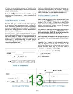
C1
SIN
aR
-S
. WIRE LVDT
R
-
R
+S
REF IN
R
+
FS = . V
aR
C.
COS
bR
R
R
.R
-C
R
R
-
.R
+C
+
. V
R
bR
+RH
-RL
C
= C , set for phase lag = phase lead through the LVDTꢀ
.
1
FIGURE 24. 2-WIRE LVDT DIRECT INPUT
15

 ETC [ ETC ]