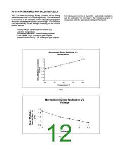
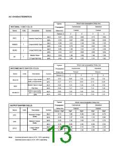
AC CHARACTERISTICS
INTERNAL CORE CELLS
Worst case propagation Delay (ns)
Typical
Commercial
Fanout
Industrial
Fanout
Propagation
Delay (ns)
Name
Cells
Description
Symbol
2
4
2
4
Fanout =2
0.27
tpLH
tpHL
tpLH
tpHL
tpLH
tpHL
0.70
0.47
1.01
0.79
1.30
0.57
0.84
0.56
1.29
1.04
1.81
0.80
0.73
0.49
1.05
0.82
1.35
0.60
0.88
0.58
1.35
1.09
1.89
0.84
INV2
1
1
1
Invertor Dual Drive
2-Input NAND Gate
2-Input NOR Gate
0.18
0.39
NAND2
NOR2
0.30
0.50
0.22
tpLH
tpHL
0.54
0.55
1.40
1.44
1.60
1.55
1.46
1.51
1.68
1.62
Master Slave
DF
1
D-Type Flip-Flop
Worst case propagation Delay (ns)
Typical
Commercial
Fanout
Industrial
Fanout
INTERMEDIATE BUFFER CELLS
Propagation
Delay (ns)
Fanout =2
Name
IBGATE
IBDF
Cells
Description
Symbol
2
4
2
4
tpLH
tpHL
0.34
0.27
0.88
0.71
1.02
0.84
0.92
0.75
1.02
0.88
Large 2 Input NAND
Gate +2 Input NOR
-
-
-
Master Slave D-type
Flip-Flop
tpLH
tpHL
0.48
0.50
1.24
1.31
1.44
1.42
1.30
1.37
1.50
1.49
CMOS input buffer
with 2 input NAND
gate
tpLH
tpLH
0.60
0.45
1.58
1.17
1.68
1.21
1.65
1.22
1.75
1.27
IBCMOS1
Typical
Worst case propagation Delay (ns)
Commercial
Fanout
Industrial
Fanout
Propagation
OUTPUT BUFFER CELLS
Delay (ns)
Name
OP3
Cells
-
Description
Symbol
Fanout =10pF
10pF
1.90
1.27
50pF
6.49
4.40
10pF
1.99
1.33
50pF
6.79
4.60
tpLH
tpHL
0.73
0.49
Standard Output
Buffer
tpHL
0.50
1.30
3.59
1.35
3.76
Medium Output
Buffer
OP6
-
-
tpLH
tpLH
0.33
0.38
0.85
0.99
2.42
2.14
0.89
1.04
2.53
2.24
Large Output
Buffer
OP12
tpHL
0.25
0.66
1.50
0.69
1.56
Note : Commercial worst case is 4.5V, 70°C operating
Industrial worst case is 4.5V, 85°C operating

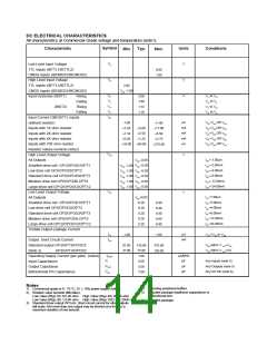
 ETC [ ETC ]