THIRD PARTY SOFTWARE SUPPORT
SPECIFICATIONS
■ Design Kits for major industry standard ASIC design
THERMAL MANAGEMENT
software tools
■ Lower power CMOS for better thermal management
■ All libraries include fully detailed timing information
■ EDIF 2.0 Interface
■ Improved reliability
■ Power packages available
■ Post layout back annotation available
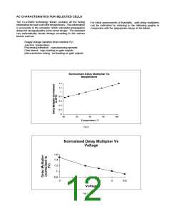
The increase in speed and density available through
CMOS process geometry reduction, results in a
corresponding increase in power dissipation. SemiCustom
designers now have the ability to design circuits of 100,000
gates and over, and chip power consumption is (or should be)
a very important concern.
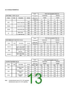
GPS supports a wide range of third party design tools
including IKOS, Mentor, Verilog, and Viewlogic at the time of
printing. Please check with our Sales Offices for the most
recent additions. The design kits offer fully detailed timing
information for all cell libraries, netlist extraction utilities, and
post layout back annotation capability where applicable. An
example of a workstation design flow is shown in fig 5 below.
Please contact your local GEC Plessey Semiconductor’s
sales office for further information about support of particular
tools.
The logic core of 100K plus gates is the dominant factor
in power dissipation at this complexity. It is essential to offer
ultra low power core logic to maintain an acceptable overall
chip power budget.
To minimize this problem GPS’s CLA70000 arrays offer
low power factors and a selection of power packages.
Dissipation of 5 µW per gate per Mhz gate power and 1µW per
gate load, is lower than most competitive arrays, with the
reduced junction temperatures having the added advantage
of improved performance and reliability.
PDS
WORKSTATION
ENVIRONMENT
ENVIRONMENT
MLE
Place &
Route
ERC &
Netlist
Schematic
Capture
Translation
Schematic
Symbols
CLA
Back -
Annotation
Libraries
Design
Verification
Simulation
Models
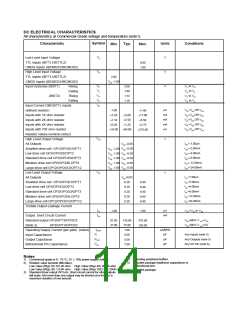
CLA70000 POWER DISSIPATION CALCULATION
Vector
Translation
CLA70000 series power dissipation for any array can be
estimated by following the example (calculated for the CLA76XXX)
below.
Simulation
Test Vector
Generation
Test Program
Generation
Number of available gates
Assume percent gates used
110112
40%
Number of used gates (110102 X 0.4)
Assume 15% of gates switching during.
each clock cycle (44045 X 0.15)
Power dissipation/gate/Mhz
44045
Fig 5. Workstation Design Flow
6607
PDS2 - THE GPS ASIC DESIGN SYSTEM
■ Behavioral, Functional, and Gate Level Modelling
■ VHDL and Third Party Links
(gate fanout typically 2 loads)
7µW
Total core dissipation/Mhz (6607 X 0.007)
Number of available I/O pads
46.2 mW
200
■ Supports Hierarchical Design Techniques
■ EDIF 2.0 Interface
Percent of I/O pads used as Outputs
Number of I/O pads used as Outputs
Number of output buffers switching
each clock cycle (20%)
40%
80
16
PDS2 is GPS’s own proprietary ASIC design system. It
provides a fully-integrated, technology independent VLSI
design environment for all GPS CMOS SemiCustom
products.
Dissipation/output buffers/Mhz/pF
Output loading
25µW
50 pF
Power/output buffer/Mhz
Total output buffer dissipation/Mhz
1.25mW
20mW
PDS2 runs on Digital Equipment Computers and is self
configuring according to the available machine resources. It
comprises design capture (schematic capture or VHDL),
testability analysis, logic simulation, fault simulation, auto
place and route, and back annotation. The system offers full
support for hierarchical design techniques, maintained from
design capture through to layout, as well as advanced design
management tools. PDS2 may be used either at a GPS
Design Center or under licence at the customer’s premises. A
three day training course is available for first time users.
Total Power dissipation/Mhz
66.2mW
Estimated dissipation of the circuit at the frequencies below is
Total Power at 10 Mhz clock rate
Total Power at 25Mhz clock rate
0.66W
1.65W

 ETC [ ETC ]