ST90158 - MULTIPROTOCOL SERIAL COMMUNICATIONS INTERFACE (SCI-M)
MULTIPROTOCOL SERIAL COMMUNICATIONS INTERFACE (Cont’d)
9.6.8 Input Signals
SIN: Serial Data Input. This pin is the serial data
input to the SCI receiver shift register.
only the data portion of the frame and its stand-by
state is high: data is valid on the rising edge of the
clock. Even in Synchronous mode CLKOUT will
only clock the data portion of the frame, but the
stand-by level and active edge polarity are pro-
grammable by the user.
TXCLK: External Transmitter Clock Input. This
pin is the external input clock driving the SCI trans-
mitter. The TXCLK frequency must be greater than
or equal to 16 times the transmitter data rate (de-
pending whether the X16 or the X1 clock have
been selected). A 50% duty cycle is required for
this input and must have a period of at least twice
INTCLK. The use of the TXCLK pin is optional.
When Synchronous mode is disabled (SMEN in
SICR is reset), the state of the XTCLK and OCLK
bits in CCR determine the source of CLKOUT; '11'
enables the Serial Expansion Mode.
RXCLK: External Receiver Clock Input. This in-
put is the clock to the SCI receiver when using an
external clock source connected to the baud rate
generator. INTCLK is normally the clock source. A
50% duty cycle is required for this input and must
have a period of at least twice INTCLK. Use of RX-
CLK is optional.
When the Synchronous mode is enabled (SMEN
in SICR is set), the state of the XTCLK and OCLK
bits in CCR determine the source of CLKOUT; '00'
disables it for PLM applications.
RTS: Request To Send. This output Alternate
Function is only enabled in Synchronous mode; it
becomes active when the Least Significant Bit of
the data frame is sent to the Serial Output Pin
(SOUT) and indicates to the target device that the
MCU is about to send a synchronous frame; it re-
turns to its stand-by value just after the last active
edge of CLKOUT (MSB transmitted). The active
level can be programmed high or low.
DCD: Data Carrier Detect. This input is enabled
only in Synchronous mode; it works as a gate for
the RXCLK clock and informs the MCU that an
emitting device is transmitting a synchronous
frame. The active level can be programmed as 1
or 0 and must be provided at least one INTCLK pe-
riod before the first active edge of the input clock.
SDS: Synchronous Data Strobe. This output Al-
ternate function is only enabled in Synchronous
mode; it becomes active high when the Least Sig-
nificant Bit is sent to the Serial Output Pins
(SOUT) and indicates to the target device that the
MCU is about to send the first bit for each synchro-
nous frame. It is active high on the first bit and it is
low for all the rest of the frame. The active level
can not be programmed.
9.6.9 Output Signals
SOUT: Serial Data Output. This Alternate Func-
tion output signal is the serial data output for the
SCI transmitter in all operating modes.
CLKOUT: Clock Output. The alternate Function
of this pin outputs either the data clock from the
transmitter in Serial Expansion or Synchronous
modes, or the clock output from the Baud Rate
Generator. In Serial expansion mode it will clock
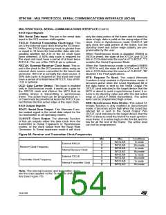
Figure 85. Receiver and Transmitter Clock Frequencies
Min
0
Max
Conditions
1x mode
INTCLK/8
INTCLK/4
INTCLK/8
INTCLK/2
INTCLK/8
INTCLK/4
INTCLK/8
INTCLK/2
External RXCLK
Receiver Clock Frequency
0
16x mode
1x mode
0
Internal Receiver Clock
0
16x mode
1x mode
0
External TXCLK
Transmitter Clock Frequency
0
16x mode
1x mode
0
Internal Transmitter Clock
0
16x mode
Note: The internal receiver and transmitter clocks
are the ones applied to the Tx and Rx shift regis-
ters (see Figure 76).
154/199
9

 ETC [ ETC ]