ST90158 - MULTIPROTOCOL SERIAL COMMUNICATIONS INTERFACE (SCI-M)
MULTIPROTOCOL SERIAL COMMUNICATIONS INTERFACE (Cont’d)
9.6.5.1 Data transfer
Data to be transmitted by the SCI is first loaded by
the program into the Transmitter Buffer Register.
The SCI will transfer the data into the Transmitter
Shift Register when the Shift Register becomes
available (empty). The Transmitter Shift Register
converts the parallel data into serial format for
transmission via the SCI Alternate Function out-
put, Serial Data Out. On completion of the transfer,
the transmitter buffer register interrupt pending bit
will be updated. If the selected word length is less
than 8 bits, the unused most significant bits do not
need to be defined.
The character match Address Interrupt mode may
be used as a powerful character search mode,
generating an interrupt on reception of a predeter-
mined character e.g. Carriage Return or End of
Block codes (Character Match Interrupt). This is
the only Address Interrupt Mode available in Syn-
chronous mode.
The Line Break condition is fully supported for both
transmission and reception. Line Break is sent by
setting the SB bit (IDPR). This causes the trans-
mitter output to be held low (after all buffered data
has been transmitted) for a minimum of one com-
plete word length and until the SB bit is Reset.
Break cannot be inserted into the transmitted
frame for the Synchronous mode.
Incoming serial data from the Serial Data Input pin
is converted into parallel format by the Receiver
Shift Register. At the end of the input data frame,
the valid data portion of the received word is trans-
ferred from the Receiver Shift Register into the Re-
ceiver Buffer Register. All Receiver interrupt con-
ditions are updated at the time of transfer. If the
selected character format is less than 8 bits, the
unused most significant bits will be set.
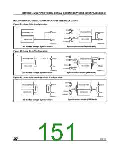
Testing of the communications channel may be
performed using the built-in facilities of the SCI pe-
ripheral. Auto-Echo mode and Loop-Back mode
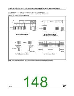
may be used individually or together. In Asynchro-
nous, Asynchronous with Synchronous Clock and
Serial Expansion modes they are available only on
SIN/SOUT pins through the programming of AEN/
LBEN bits in CCR. In Synchronous mode (SMEN
set) the above configurations are available on SIN/
SOUT, RXCLK/CLKOUT and DCD/RTS pins by
programming the AEN/LBEN bits and independ-
ently of the programmed polarity. In the Synchro-
nous mode case, when AEN is set, the transmitter
outputs (data, clock and control) are disconnected
from the I/O pins, which are driven directly by the
receiver input pins (Auto-Echo mode: SOUT=SIN,
CLKOUT=RXCLK and RTS=DCD, even if they act
on the internal receiver with the programmed po-
larity/edge). When LBEN is set, the receiver inputs
(data, clock and controls) are disconnected and
the transmitter outputs are looped-back into the re-
ceiver section (Loop-Back mode: SIN=SOUT, RX-
CLK=CLKOUT, DCD=RTS. The output pins are
locked to their programmed stand-by level and the
status of the INPL, XCKPL, DCDPL, OUTPL,
OCKPL and RTSPL bits in the SICR register are ir-
relevant). Refer to Figure 81, Figure 82, and Fig-
ure 83 for these different configurations.
The Frame Control and Status block creates and
checks the character configuration (Data length
and number of Stop bits), as well as the source of
the transmitter/receiver clock.
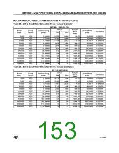
The internal Baud Rate Generator contains a pro-
grammable divide by “N” counter which can be
used to generate the clocks for the transmitter
and/or receiver. The baud rate generator can use
INTCLK or the Receiver clock input via RXCLK.
The Address bit/D9 is optional and may be added
to any word in Asynchronous and Serial Expan-
sion modes. It is commonly used in network or ma-
chine control applications. When enabled (AB set),
an address or ninth data bit can be added to a
transmitted word by setting the Set Address bit
(SA). This is then appended to the next word en-
tered into the (empty) Transmitter Buffer Register
and then cleared by hardware. On character input,
a set Address Bit can indicate that the data pre-
ceding the bit is an address which may be com-
pared in hardware with the value in the Address
Compare Register (ACR) to generate an Address
Match interrupt when equal.
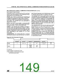
Table 27. Address Interrupt Modes
(1)
The Address bit and Address Comparison Regis-
ter can also be combined to generate four different
types of Address Interrupt to suit different proto-
cols, based on the status of the Address Mode En-
able bit (AMEN) and the Address Mode bit (AM) in
the CHCR register.
If 9th Data Bit is set
If Character Match
(1)
If Character Match and 9th Data Bit is set
(1)
If Character Match Immediately Follows BREAK
(1)
Not available in Synchronous mode
150/199
9

 ETC [ ETC ]