ST90158 - GENERAL DESCRIPTION
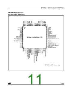
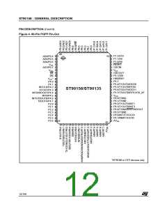
1.2 PIN DESCRIPTION
RESET: Reset (input, active low). The ST9 is ini-
tialised by the Reset signal. With the deactivation
of RESET, program execution begins from the
memory location pointed to by the vector con-
tained in memory locations 00h and 01h.
OSCIN, OSCOUT: Oscillator (input and output).
These pins connect a parallel-resonant crystal (3
to 5 MHz), or an external source to the on-chip
clock oscillator and buffer. OSCIN is the input of
the oscillator inverter and internal clock generator;
OSCOUT is the output of the oscillator inverter.
AS: Address Strobe (output, active low, 3-state).
Address Strobe is pulsed low once at the begin-
ning of each memory cycle. The rising edge of AS
indicates that address, Read/Write (R/W), and
Data Memory signals are valid for memory trans-
fers. Under program control, AS can be placed in a
high-impedance state along with Port 0, Port 1 and
Data Strobe (DS). AS is active after reset on Rom-
less device.
HW0_SW1: When connected to V through a 1K
DD
pull-up resistor, the software watchdog option is
selected. When connected to V
through a 1K
SS
pull-down resistor, the hardware watchdog option
is selected.
V
: Programming voltage for EPROM/OTP de-
PP
vices. Must be connected to V
through a 10 Kohm resistor.
in user mode
SS
DS: Data Strobe (output, active low, 3-state). Data
Strobe provides the timing for data movement to or
from Port 0 for each memory transfer. During a
write cycle, data out is valid at the leading edge of
DS. During a read cycle, Data In must be valid pri-
or to the trailing edge of DS. When the ST90158
accesses on-chip memory, DS is held high during
the whole memory cycle. It can be placed in a high
impedance state along with Port 0, Port 1 and AS.
DS is active after reset on Romless device.
AV : Analog V
verter.
of the Analog to Digital Con-
DD
DD
AV : Analog V of the Analog to Digital Con-
SS
SS
verter.
V
V
: Main Power Supply Voltage.
DD
: Digital Circuit Ground.
SS
P0[7:0], P1[7:0]: (Input/Output, TTL or CMOS
compatible). 16 lines grouped into I/O ports provid-
ing the external memory interface for addressing
64Kbytes of external memory.
R/W: Read/Write (output, 3-state). Read/Write de-
termines the direction of data transfer for external
memory transactions. R/W is low when writing to
external memory, and high for all other transac-
tions. It can be placed in high impedance state
along with Port 0, Port 1, AS and DS. R/W is not
active after reset on Romless device.
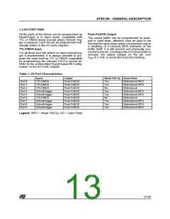
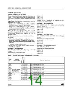
P0[7:0], P1[7:0], P2[6:0], P4[7:0], P5[7:3], P5.1,
P6[6:0], P7[7:0], P8[7:0], P9[7:4], P9[2:0]: I/O
Port Lines (Input/Output, TTL or CMOS compati-
ble). I/O lines grouped into I/O ports of 8 bits, bit
programmable under program control as general
purpose I/O or as alternate functions.
10/199
9

 ETC [ ETC ]