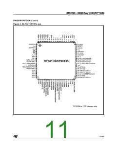
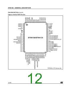
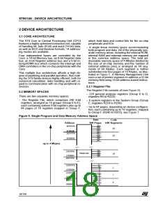
ST90158 - GENERAL DESCRIPTION
I/O PORT PINS (Cont’d)
How to Configure the I/O ports
To configure the I/O ports, use the information in
Table 1, Table 2 and the Port Bit Configuration Ta-
ble (Table 19) in the I/O Ports Chapter (See page
91).
Input Note = the hardware characteristics fixed for
each port line in Table 1.
P9C2.5=1
P9C1.5=0
P9C0.5=1
Enable the SCI peripheral by software as de-
scribed in the SCI chapter.
Example 2: SCI data output
– If Input note = TTL/CMOS, either TTL or CMOS
input level can be selected by software.
AF: S0OUT, Port: P9.4 Output push-pull (config-
ured by software).
– If Input note = Schmitt trigger, selecting CMOS
or TTL input by software has no effect, the input
will always be Schmitt Trigger.
Write the port configuration bits:
P9C2.4=0
Alternate Functions (AF) = More than one AF
cannot be assigned to an I/O pin at the same time.
All alternate functions are mapped on Port 2
through Port 9.
P9C1.4=1
P9C0.4=1
Example 3: ADC data input
AF: AIN0, Port : P7.0, Input Note: does not apply
to ADC
An alternate function can be selected as follows.
AF Inputs:
Write the port configuration bits:
P7C2.0=1
– AF is selected implicitly by enabling the corre-
sponding peripheral. Exception to this are A/D
inputs which must be explicitly selected as AF by
software.
P7C1.0=1
P7C0.0=1
AF Outputs or Bidirectional Lines:
Example 4: External Memory I/O
AF: AD0, Port : P0.0
Write the port configuration bits:
P0C2.0=0
– In the case of Outputs or I/Os, AF is selected
explicitly by software.
Example 1: SCI data input
AF: S0IN, Port: P9.5, Port Style: Input Schmitt
Trigger.
P0C1.0=1
Write the port configuration bits:
P0C0.0=1
Table 2. I/O Port Description and Alternate Functions
Pin
No.
Port
General
Alternate Functions
Purpose I/O
Name
P0.0
P0.1
P0.2
P0.3
P0.4
P0.5
P0.6
P0.7
P1.0
P1.1
75 77 AD0
76 78 AD1
77 79 AD2
78 80 AD3
I/O Address/Data bit 0 mux
I/O Address/Data bit 1 mux
I/O Address/Data bit 2 mux
I/O Address/Data bit 3 mux
I/O Address/Data bit 4 mux
I/O Address/Data bit 5 mux
I/O Address/Data bit 6 mux
I/O Address/Data bit 7 mux
I/O Address bit 8
All ports useable
for general pur-
pose I/O (input,
output or bidirec-
tional)
79
80
1
1
2
3
5
AD4
AD5
AD6
AD7
3
60 62 A8
61 63 A9
I/O Address bit 9
14/199
9

 ETC [ ETC ]