ST72104G, ST72215G, ST72216G, ST72254G
SUPPLY CURRENT CHARACTERISTICS (Cont’d)
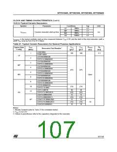
14.4.2 WAIT and SLOW WAIT Modes
1)
2)
Symbol
Parameter
Conditions
Typ
Max
Unit
150
560
2200
280
900
3000
f
f
f
=1MHz, f
=500kHz
=2MHz
=8MHz
3)
OSC
OSC
OSC
CPU
Supply current in WAIT mode
(see Figure 61)
=4MHz, f
CPU
=16MHz, f
CPU
20
90
340
70
190
850
f
f
f
=1MHz, f
=31.25kHz
=125kHz
=500kHz
4)
4)
OSC
OSC
OSC
CPU
Supply current in SLOW WAIT mode
(see Figure 62)
=4MHz, f
=16MHz, f
CPU
CPU
I
µA
DD
90
350
1370
200
550
1900
f
f
f
=1MHz, f
=500kHz
=2MHz
=8MHz
3)
OSC
OSC
OSC
CPU
Supply current in WAIT mode
=4MHz, f
CPU
(see Figure 61)
=16MHz, f
CPU
10
50
200
20
80
350
f
f
f
=1MHz, f
=31.25kHz
=125kHz
=500kHz
OSC
OSC
OSC
CPU
Supply current in SLOW WAIT mode
(see Figure 62)
=4MHz, f
CPU
=16MHz, f
CPU
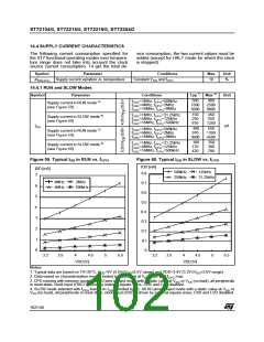
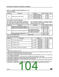
Figure 61. Typical I in WAIT vs. f
Figure 62. Typical I in SLOW-WAIT vs. f
DD
CPU
DD
CPU
IDD [mA]
IDD [mA]
8MHz
4MHz
2MHz
500kHz
500kHz
250kHz
125kHz
3
2.5
2
0.35
31.25kHz
0.3
0.25
0.2
1.5
1
0.15
0.1
0.5
0
0.05
0
3.2
3.5
4
4.5
5
5.5
3.2
3.5
4
4.5
5
5.5
VDD [V]
VDD [V]
Notes:
1. Typical data are based on T =25°C, V =5V (4.5V≤V ≤5.5V range) and V =3.4V (3.2V≤V ≤3.6V range).
A
DD
DD
DD
DD
2. Data based on characterization results, tested in production at V max. and f
max.
DD
CPU
3. All I/O pins in input mode with a static value at V or V (no load), all peripherals in reset state; clock input (OSC1)
DD
SS
driven by external square wave, CSS and LVD disabled.
4. SLOW-WAIT mode selected with f
based on f
divided by 32. All I/O pins in input mode with a static value at
OSC
CPU
V
or V (no load), all peripherals in reset state; clock input (OSC1) driven by external square wave, CSS and LVD
DD
SS
disabled.
103/140

 ETC [ ETC ]