ST72104G, ST72215G, ST72216G, ST72254G
OPERATING CONDITIONS (Cont’d)
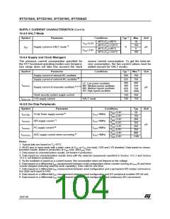
14.3.2 Operating Conditions with Low Voltage Detector (LVD)
Subject to general operating conditions for V , f
, and T .
A
DD OSC
Conditions
High Threshold
1)
Symbol
Parameter
Min
Typ
Max
Unit
2)
4.10
3.75
3.25
4.30
3.90
3.35
4.50
4.05
3.55
Reset release threshold
2)
2)
V
Med. Threshold
Low Threshold
IT+
(V rise)
DD
V
2)
2)
High Threshold
Med. Threshold
Low Threshold
3.85
3.50
4.05
3.65
3.10
4.30
3.95
3.35
Reset generation threshold
V
V
IT-
(V fall)
4)
DD
3.00
200
0.2
LVD voltage threshold hysteresis
V
-V
250
300
50
mV
V/ms
ns
hyst
IT+ IT-
3)
Vt
V
rise time rate
POR
DD
2)
t
Filtered glitch delay on V
Not detected by the LVD
40
g(VDD)
DD
3)
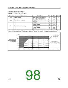
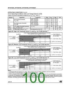
Figure 53. High LVD Threshold Versus VDD and f
for FLASH devices
OSC
FUNCTIONALITY AND RESET NOT GUARANTEED IN THIS AREA
FOR TEMPERATURES HIGHER THAN 85°C
f
[MHz]
FUNCTIONALITY
NOT GUARANTEED
IN THIS AREA
OSC
16
DEVICE UNDER
RESET
12
IN THIS AREA
FUNCTIONAL AREA
8
0
SUPPLY VOLTAGE [V]
V
≥3.85
IT-
2.5
3
3.5
4
4.5
5
5.5
3)
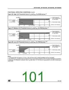
Figure 54. Medium LVD Threshold Versus VDD and f
for FLASH devices
OSC
FUNCTIONALITY AND RESET NOT GUARANTEED IN THIS AREA
FOR TEMPERATURES HIGHER THAN 85°C
f
[MHz]
FUNCTIONALITY
NOT GUARANTEED
IN THIS AREA
OSC
16
DEVICE UNDER
RESET
12
IN THIS AREA
FUNCTIONAL AREA
8
0
SUPPLY VOLTAGE [V]
2.5
3
V
IT-≥3.5V
4
4.5
5
5.5
2)4)
Figure 55. Low LVD Threshold Versus VDD and f
for FLASH devices
OSC
FUNCTIONALITY NOT GUARANTEED IN THIS AREA
FOR TEMPERATURES HIGHER THAN 85°C
f
[MHz]
FUNCTIONALITY
NOT GUARANTEED
IN THIS AREA
OSC
16
12
DEVICE UNDER
RESET
IN THIS AREA
FUNCTIONAL AREA
8
SEE NOTE 4
0
SUPPLY VOLTAGE [V]
2.5
V
IT-≥3V 3.2
3.5
4
4.5
5
5.5
Notes:
1. LVD typical data are based on T =25°C. They are given only as design guidelines and are not tested.
A
2. Data based on characterization results, not tested in production.
3. The V rise time rate condition is needed to insure a correct device power-on and LVD reset. Not tested in production.
DD
4. If the low LVD threshold is selected, when V falls below 3.2V, (V minimum operating voltage), the device is guar-
DD
DD
anteed to continue functioning until it goes into reset state. The specified V min. value is necessary in the device power
DD
on phase, but during a power down phase or voltage drop the device will function below this min. level.
100/140

 ETC [ ETC ]