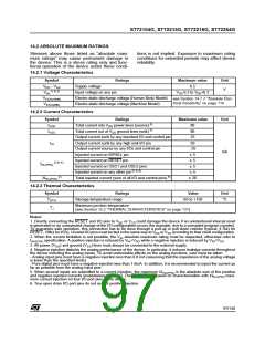
ST72104G, ST72215G, ST72216G, ST72254G
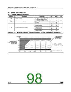
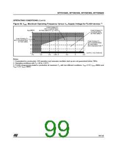
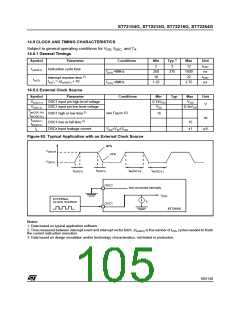
FUNCTIONAL OPERATING CONDITIONS (Cont’d)
2)
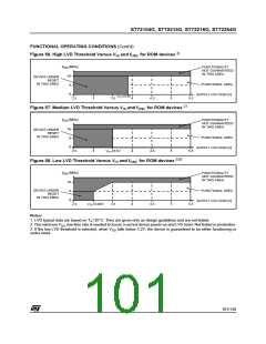
Figure 56. High LVD Threshold Versus VDD and f
for ROM devices
OSC
f
[MHz]
FUNCTIONALITY
NOT GUARANTEED
IN THIS AREA
OSC
16
DEVICE UNDER
RESET
IN THIS AREA
FUNCTIONAL AREA
8
0
SUPPLY VOLTAGE [V]
V
≥3.85
IT-
2.5
3
3.5
4
4.5
5
5.5
5.5
5.5
2)
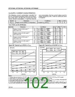
Figure 57. Medium LVD Threshold Versus VDD and f
for ROM devices
OSC
f
[MHz]
FUNCTIONALITY
NOT GUARANTEED
IN THIS AREA
OSC
16
DEVICE UNDER
RESET
IN THIS AREA
FUNCTIONAL AREA
8
0
SUPPLY VOLTAGE [V]
2.5
3
V
IT-≥3.5V
4
4.5
5
2)3)
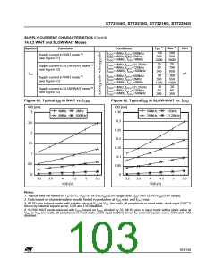
Figure 58. Low LVD Threshold Versus VDD and f
for ROM devices
OSC
f
[MHz]
FUNCTIONALITY
NOT GUARANTEED
IN THIS AREA
OSC
16
DEVICE UNDER
RESET
IN THIS AREA
FUNCTIONAL AREA
8
0
SUPPLY VOLTAGE [V]
2.5
V
IT-≥3.00V
3.5
4
4.5
5
Notes:
1. LVD typical data are based on T =25°C. They are given only as design guidelines and are not tested.
A
2. The minimum V rise time rate is needed to insure a correct device power-on and LVD reset. Not tested in production.
DD
3. If the low LVD threshold is selected, when V falls below 3.2V, the device is guaranteed to be either functioning or
DD
under reset.
101/140

 ETC [ ETC ]