®
PMD-100
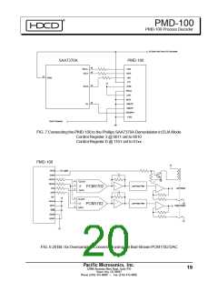
PMD-100 Process Decoder
Additional PMD-100 Considerations
Power and Ground
VDD1 (pin 7) powers the core. VDD2 (pin 22) powers the output pins. VDD1 may be connected to VDD2 externally.
For lowest output clock jitter, it is recommended that VDD2 be powered from it’s own separately regulated power supply.
VSS1 (pin 8) and VSS2 (pin 21) are internally connected and must be externally connected to the same ground source.
Adding a 0.1uF capacitor on each VDD-VSS pair, as close to these pins as possible, is strongly recommended.
Input Pins
Some of the input pins, such as HMUTE (pin 17) can produce several 10’s of microamps of noise current when pulled low.
Because these inputs have TTL compatible input thresholds, this current can produce false triggering of logic high unless
the impedance to ground is less than 1000 ohms. If these inputs are driven by logic or pulled low to ground with a switch,
there is no problem.
Serial Data Input
Due to the high-speed characteristics of the PMD-100, care should be taken to minimize high-frequency noise on the serial
data and clock inputs. The PMD-100 operates at TTL level thresholds and even very narrow spikes over 0.5V may be
interpreted as valid data. Input data to the PMD-100 should be properly terminated, either by series termination at the
source, or if necessary, AC termination at the PMD-100 input. Series termination may be especially helpful for the master
clock source, XTI. A 100 ohm resistor in series with the XTI signal, as close to the source as possible, will help to prevent
undershoot and potential lock-up. Also, pay close attention to the timing relationship of XTI relative to LRCI.
Output Clocking
Although every effort has been made to keep the internally generated jitter low in the PMD-100, for the best sonic
performance we recommend re-clocking the critical conversion clock(s) using external circuitry. Don’t forget to maintain
the timing relationships of the word clock, bit clock, and the right and left data outputs. The simplest thing to do is to just
re-clock all of these output signals. When used as a low jitter filter without external re-clocking, the PMD-100 should
have its own power regulator and a 10uf in parallel with a 0.1uf decoupling capacitor for each power pin. Although the
PMD-100 accepts either 256 or 384 Fs, it’s output timing is based upon a 256 Fs system clock with a changing duty cycle.
The PMD-100 incorporates the Patented “Silent Conversion” variable clock timing and was designed to output a very
stable word clock. These features resulted in minimizing jitter induced sonic degradation. However, the PMD-100 was
designed prior to the introduction of bit clocked DACs. Therefore, additional care must be used when implementing the
PMD-100 and any bit clocked DAC. In general, the PMD-100 exhibits more jitter on it’s bit clock output when
compared to it’s word clock output.
The PMD-100’s internally generated jitter on the bit clock output is lower when it is operated at 256 Fs when compared
to 384 Fs (XTIM low versus high). When implementing the PMD-100 into a 384 Fs and bit clocked DAC design, we
strongly recommend using re-clocking circuitry in order to attain the best possible sonic perfomance. To assure jitter-free
conversion, digital signals should be reclocked directly from an oscillator placed near the DAC(s). By selecting a 768 Fs
system clock to synchronize the re-clocking circuitry, then divide the system clock by two (using a flip-flop) which yields
the desired 384 Fs system clock to drive the rest of the circuitry. For additional details on this implementation of the
PMD-100, please contact Pacific Microsonics.
Pacific Microsonics, Inc.
15
32990 Alvarado Niles Road, Suite 910
Union City, CA 94587
Phone (510) 475-8000
Fax (510) 475-8005

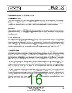
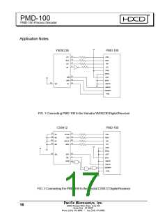
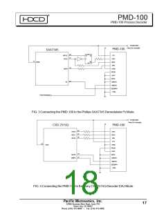
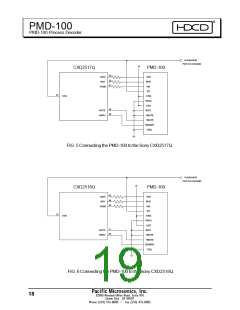
 ETC [ ETC ]