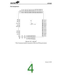
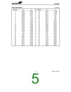
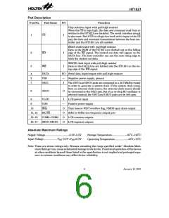
HT1621
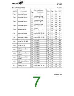
A.C. Characteristics
Ta=25°C
Test Conditions
Conditions
Symbol
Parameter
Min.
Typ.
Max. Unit
VDD
fSYS1
System Clock
3V On-chip RC oscillator
5V
256
256
kHz
kHz
kHz
kHz
kHz
kHz
Hz
¾
¾
¾
¾
¾
¾
¾
¾
¾
¾
¾
¾
¾
¾
¾
¾
¾
¾
¾
¾
¾
¾
¾
¾
¾
3V
Crystal oscillator
5V
32.768
32.768
256
fSYS2
System Clock
System Clock
3V
External clock source
5V
fSYS3
256
fSYS1/1024
On-chip RC oscillator
Crystal oscillator
¾
¾
fLCD
f
SYS2/128
LCD Clock
Hz
f
SYS3/1024
External clock source
n: Number of COM
Hz
¾
tCOM
fCLK1
n/fLCD
¾
LCD Common Period
s
¾
3V
5V
3V
5V
¾
150 kHz
300 kHz
Serial Data Clock (WR pin)
Duty cycle 50%
Duty cycle 50%
¾
75
kHz
¾
fCLK2
Serial Data Clock (RD pin)
150 kHz
¾
fTONE
Tone Frequency
On-chip RC oscillator
CS
2.0 or 4.0
kHz
ns
¾
¾
Serial Interface Reset Pulse
(Figure 3)
tCS
250
¾
¾
Width
Write mode
Read mode
Write mode
Read mode
3.34
6.67
1.67
3.34
¾
¾
¾
¾
¾
¾
¾
¾
3V
ms
ms
ns
ns
ns
ns
ns
WR, RD Input Pulse Width
(Figure 1)
tCLK
5V
3V
5V
3V
5V
3V
5V
3V
5V
3V
5V
Rise/Fall Time Serial Data
(Figure 1)
tr, tf
120
120
120
100
100
¾
¾
¾
¾
¾
¾
¾
¾
¾
¾
¾
¾
¾
¾
¾
Clock Width
Setup Time for DATA to WR,
RD Clock Width (Figure 2)
tsu
Hold Time for DATA to WR,
RD Clock Width (Figure 2)
th
Setup Time for CS to WR, RD
(Figure 3)
tsu1
Clock Width
Hold Time for CS to WR, RD
Clock Width (Figure 3)
th1
8
January 10, 2001

 ETC [ ETC ]