HT1621
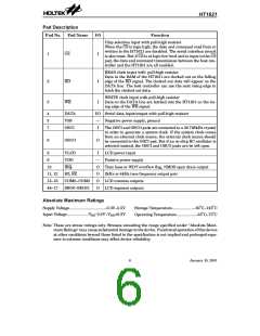
Pad Description
Pad No.
Pad Name
I/O
Function
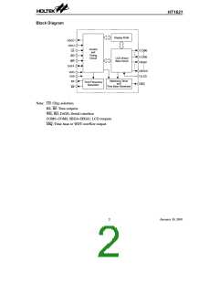
Chip selection input with pull-high resistor
When the CS is logic high, the data and command read from or
written to the HT1621 are disabled. The serial interface circuit
is also reset. But if CS is at logic low level and is input to the CS
pad, the data and command transmission between the host con-
troller and the HT1621 are all enabled.
1
CS
I
READ clock input with pull-high resistor
Data in the RAM of the HT1621 are clocked out on the falling
edge of the RD signal. The clocked out data will appear on the
DATA line. The host controller can use the next rising edge to
latch the clocked out data.
2
3
RD
I
I
WRITE clock input with pull-high resistor
Data on the DATA line are latched into the HT1621 on the ris-
ing edge of the WR signal.
WR
4
5
7
DATA
VSS
I/O Serial data input/output with pull-high resistor
Negative power supply, ground
¾
OSCI
I
The OSCI and OSCO pads are connected to a 32.768kHz crystal
in order to generate a system clock. If the system clock comes
from an external clock source, the external clock source should
be connected to the OSCI pad. But if an on-chip RC oscillator is
selected instead, the OSCI and OSCO pads can be left open.
6
OSCO
O
8
VLCD
I
LCD power input
9
VDD
Positive power supply
¾
O
O
O
O
10
IRQ
Time base or WDT overflow flag, NMOS open drain output
2kHz or 4kHz tone frequency output pair
LCD common outputs
11, 12
13~16
48~17
BZ, BZ
COM0~COM3
SEG0~SEG31
LCD segment outputs
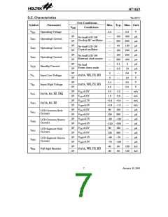
Absolute Maximum Ratings
Storage Temperature....................-50oC~125oC
Operating Temperature..................-25oC~75oC
Supply Voltage.................................-0.3V~5.5V
Input Voltage....................VSS-0.3V~VDD+0.3V
Note: These are stress ratings only. Stresses exceeding the range specified under ²Absolute Maxi-
mum Ratings² may cause substantial damage to the device. Functional operation of this device
at other conditions beyond those listed in the specification is not implied and prolonged expo-
sure to extreme conditions may affect device reliability.
6
January 10, 2001

 ETC [ ETC ]