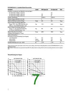
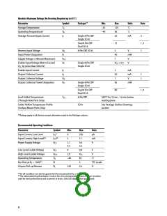
Absolute Maximum Ratings (No Derating Required up to 85˚C)
Parameter
Symbol
Package**
Min.
–55
–40
Max.
125
85
Units
˚C
Note
Storage Temperature
Operating Temperature†
Average Forward Input Current
TS
TA
IF
˚C
Single 8-Pin DIP
Single SO-8
20
mA
2
Dual 8-Pin DIP
Dual SO-8
15
1, 3
1
Reverse Input Voltage
VR
PI
8-Pin DIP, SO-8
5
V
Input Power Dissipation
40
mW
V
Supply Voltage (1 Minute Maximum)
VCC
VE
7
Enable Input Voltage (Not to Exceed
VCC by more than 500 mV)
Single 8-Pin DIP
Single SO-8
VCC + 0.5
V
Enable Input Current
IE
5
mA
mA
V
Output Collector Current
Output Collector Voltage
Output Collector Power Dissipation
IO
50
7
1
1
VO
PO
Single 8-Pin DIP
Single SO-8
85
mW
Dual 8-Pin DIP
Dual SO-8
60
1, 4
Lead Solder Temperature
(Through Hole Parts Only)
TLS
8-Pin DIP
260˚C for 10 sec., 1.6 mm below
seating plane
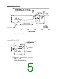
Solder Reflow Temperature Profile
(Surface Mount Parts Only)
SO-8
See Package Outline Drawings
section
**Ratings apply to all devices except otherwise noted in the Package column.
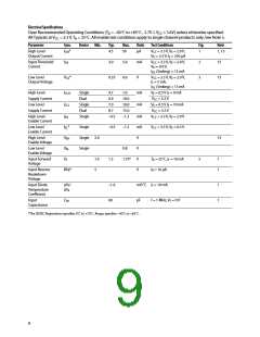
Recommended Operating Conditions
Parameter
Symbol
Min.
0
Max.
250
15
Units
µA
Input Current, Low Level
Input Current, High Level[1]
Power Supply Voltage
IFL*
IFH**
VCC
5
mA
V
2.7
4.5
3.6
5.5
Low Level Enable Voltage
High Level Enable Voltage
Operating Temperature
Fan Out (at RL = 1 kΩ)[1]
Output Pull-up Resistor
VEL
VEH
TA
0
0.8
VCC
85
5
V
2.0
–40
V
˚C
N
TTL Loads
Ω
RL
330
4 k
*The off condition can also be guaranteed by ensuring that V ≤ 0.8 volts.
FL
**The initial switching threshold is 5 mA or less. It is recommended that 6.3 mA to 10 mA be
used for best performance and to permit at least a 20% LED degradation guardband.
8

 ETC [ ETC ]