Application Information
Common-Mode Rejection for HCPL-260L Families:
Also, common-mode transients can capacitively cou-
ple from the LED anode (or cathode) to the output-side
ground causing current to be shunted away from the
LED (which can be bad if the LED is on) or conversely
cause current to be injected into the LED (bad if the LED
is meant to be off). Figure 14 shows the parasitic capaci-
tances which exists between LED anode/cathode and
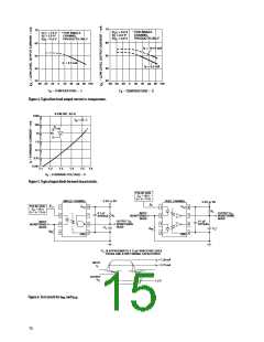
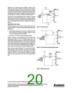
Figure 13 shows the recommended drive circuit for op-
timal common-mode rejection performance. Two main
points to note are:
1. The enable pin is tied to V rather than floating (this
CC
applies to single-channel parts only).
2. Two LED-current setting resistors are used instead of
one. This is to balance I
mode transients.
variation during common-
LED
output ground (C and C ). Also shown in Figure 14 on
LA
LC
the input side is an AC-equivalent circuit.
If the enable pin is left floating, it is possible for common-
mode transients to couple to the enable pin, resulting in
common-mode failure. This failure mechanism only oc-
curs when the LED is on and the output is in the Low
State. It is identified as occurring when the transient out-
put voltage rises above 0.8 V. Therefore, the enable pin
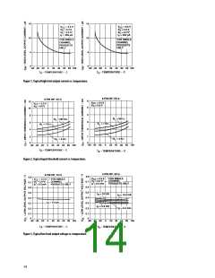
For transients occurring when the LED is on, common-
mode rejection (CMR , since the output is in the “low”
L
state) depends upon the amount of LED current drive
(I ). For conditions where I is close to the switching
F
F
threshold (I ), CMR also depends on the extent which
TH
L
I
and I balance each other. In other words, any condi-
LP
LN
should be connected to either V or logic-level high for
CC
tion where common-mode transients cause a momen-
best common-mode performance with the output low
tary decrease in I will cause common-mode failure for
F
(CMR ). This failure mechanism is only present in single-
L
transients which are fast enough.
channel parts which have the enable function.
HCPL-260L
*
1
8
7
V
V
CC
CC+
0.01 µF
220 Ω
220 Ω
350 Ω
2
3
4
6
5
V
O
74LS04
OR ANY TOTEM-POLE
OUTPUT LOGIC GATE
GND
SHIELD
*
GND1
GND2
* HIGHER CMR MAY BE OBTAINABLE BY CONNECTING PINS 1, 4 TO INPUT GROUND (GND1).
Figure 13. Recommended drive circuit for High-CMR.
1
2
8
7
V
V
+
CC
1/2 R
1/2 R
0.01 µF
LED
350 Ω
I
LP
LED
C
I
LA
LN
3
4
6
5
O
15 pF
C
LC
GND
SHIELD
+
–
V
CM
Figure 14. AC equivalent circuit.
19

 ETC [ ETC ]