Package Characteristics
All Typicals at T = 25˚C.
A
Parameter
Sym.
Package
Min. Typ.
Max
Units
Test Conditions
Fig. Note
Input-Output
Insulation
II-O*
Single 8-Pin DIP
Single SO-8
1
µA
45% RH, t = 5 s,
16, 17
VI-O = 3 kV DC, TA = 25˚C
Input-Output
Momentary
Withstand
Voltage**
VISO
8-Pin DIP, SO-8
3750
V rms
RH ≤ 50%, t = 1 min,
TA = 25˚C
16, 17
Input-Output
Resistance
RI-O
CI-O
II-I
8-Pin, SO-8
1012
0.6
Ω
VI-O =500 V dc
1, 16, 19
1, 16, 19
20
Input-Output
Capacitance
8-Pin DIP, SO-8
Dual Channel
pF
µA
f = 1 MHz, TA = 25˚C
Input-Input
Insulation
Leakage
0.005
RH ≤ 45%, t = 5 s,
V
I-I = 500 V
Current
Resistance
(Input-Input)
RI-I
CI-I
Dual Channel
1011
Ω
20
20
Capacitance
(Input-Input)
Dual 8-Pin Dip
Dual SO-8
0.03
0.25
pG
f = 1 MHz
*The JEDEC Registration specifies 0˚C to +70˚C. Avago specifies –40˚C to +85˚C.
**The Input-Output Momentary Withstand Voltage is a dielectric voltage rating that should not be interpreted as an input-output continuous
voltage rating. For the continuous voltage rating refer to the IEC/EN/DIN EN 60747-5-2 Insulation Characteristics Table (if applicable), your equip-
ment level safety specification or Avago Application Note 1074 entitled "Optocoupler Input-Output Endurance Voltage."
Notes:
1. Each channel.
2. Peaking circuits may produce transient input currents up to 50 mA, 50 ns maximum pulse width, provided average current does not
exceed 20 mA.
3. Peaking circuits may produce transient input currents up to 50 mA, 50 ns maximum pulse width, provided average current does not
exceed 15 mA.
4. Derate linearly above +80˚C free-air temperature at a rate of 2.7 mW/˚C for the SOIC-8 package.
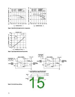
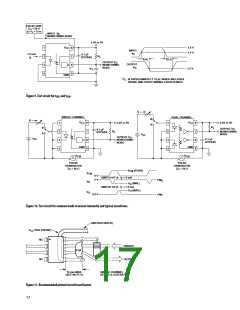
5. Bypassing of the power supply line is required, with a 0.1 µF ceramic disc capacitor adjacent to each optocoupler as illustrated in
Figure 11. Total lead length between both ends of the capacitor and the isolator pins should not exceed 20 mm.
6. The t
propagation delay is measured from the 3.75 mA point on the falling edge of the input pulse to the 1.5 V point on the rising edge
PLH
of the output pulse.
7. The t
propagation delay is measured from the 3.75 mA point on the rising edge of the input pulse to the 1.5 V point on the falling edge
PHL
of the output pulse.
8. t is equal to the worst case difference in t
and/or t
that will be seen between units at any given temperature and specified test
PSK
PHL
PLH
conditions.
9. See test circuit for measurement details.
10. The t
enable propagation delay is measured from the 1.5 V point on the falling edge of the enable input pulse to the 1.5 V point on the
ELH
rising edge of the output pulse.
11. The t enable propagation delay is measured from the 1.5 V point on the rising edge of the enable input pulse to the 1.5 V point on the
ELH
falling edge of the output pulse.
12. CM is the maximum tolerable rate of rise on the common mode voltage to assure that the output will remain in a high logic state
H
(i.e., V > 2.0 V).
o
13. CM is the maximum tolerable rate of fall of the common mode voltage to assure that the output will remain in a low logic state
L
(i.e., V < 0.8 V).
14. For sinusoidal voltages, (|dV | / dt)
o
= πf
V
(p-p).
CM
max
CM CM
15. No external pull up is required for a high logic state on the enable input. If the V pin is not used, tying V to V will result in improved
E
E
CC
CMR performance. For single channel products only. See application information provided.
16. Device considered a two-terminal device: pins 1, 2, 3, and 4 shorted together, and pins 5, 6, 7, and 8 shorted together.
17. In accordance with UL 1577, each optocoupler is proof tested by applying an insulation test voltage ≥ 4500 V rms for one second (leakage
detection current limit, I ≤ 5 µA). This test is performed before the 100% production test for partial discharge (Method b) shown in the
I-O
IEC/EN/DIN EN 60747-5-2 Insulation Characteristics Table, if applicable.
18. In accordance with UL 1577, each optocoupler is proof tested by applying an insulation test voltage ≥ 6000 V rms for one second (leakage
detection current limit, I ≤ 5 µA). This test is performed before the 100% production test for partial discharge (Method b) shown in the
I-O
IEC/EN/DIN EN 60747-5-2 Insulation Characteristics Table, if applicable.
19. Measured between the LED anode and cathode shorted together and pins 5 through 8 shorted together. For dual channel products only.
20. Measured between pins 1 and 2 shorted together, and pins 3 and 4 shorted together. For dual channel products only.
13

 ETC [ ETC ]