HY6264A Series
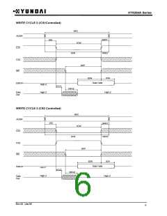
Notes(Write Cycle):
1. A write occurs during the overlap of a low /CS1 and high CS2 and a low /WE. A write begins at the latest
transition among /CS1 going low, CS2 going high and /WE going low: A write ends at the earliest
transition among /CS1 going high, CS2 going low and /WE going high. tWP is measured from the
beginning of write to the end of write.
2. tCW is measured from the later of /CS1 going low or CS2 going high to end of write.
3. tAS is measured from the address valid to the beginning of write.
4. tWR is measured from the end of write to the address change. tWR1 is applied in case a write ends as
/CS1, or /WE going high, and tWR2 is applied in case a write ends at CS2 going low.
5. If /OE, CS2 and /WE are in the read mode during this period, and the I/O pins are in the output low-Z
state, inputs of opposite phase of the output must not be applied because bus contention can occur.
6. If /CS1 goes low simultaneously with /WE going low or after /WE going low, the outputs remain high
impedance state.
7. DOUT is the read data of the new address.
8. When /CS1 is low and CS2 is high,I /O pins are in the output state. The input signals in the opposite
phase leading to the outputs should not be applied.
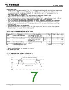
DATA RETENTION CHARACTERISTICS.
Symbol
Parameter
Test Condition
Min
Typ
Max
Unit
VDR
Vcc for Data Retention
2
-
-
V
/CS1>Vcc-0.2V, CS2¡ 0Â.2V
or>Vcc-0.2V, Vss<VIN<Vcc
Vcc = 3.0V, /CS1>Vcc-0.2V
CS2<0.2V or >Vcc-0.2V
Vss<VIN<Vcc
ICCDR
Data Retention Current
L
LL
-
-
1
1
50
5
uA
uA
tCDR
tR
Chip Disable to Data
Retention Time
Operating Recovery Time
See Data Retention Timing
Diagram
0
-
-
-
-
ns
ns
tRC(2)
Note
1.Typical values are under the condition of TA=25°C.
2.tRC is read cycle time
DATA RETENTION TIMING DIAGRAM 1
DATA RETENTION MODE
VCC
4.5V
tCDR
tR
2.2V
VDR
CS1>VCC-0.2V
CS1
VSS
Rev.02 /Jan.99
7

 ETC [ ETC ]