HY6264A Series
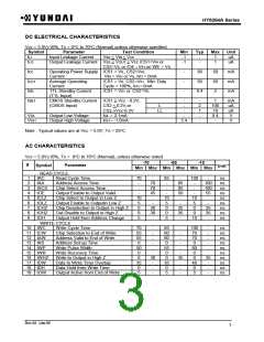
DC ELECTRICAL CHARACTERISTICS
Vcc = 5.0V±10%, TA = 0°C to 70°C (Normal) unless otherwise specified
Symbol
ILI
ILO
Parameter
Input Leakage Current
Output Leakage Current Vss < VOUT < Vcc /CS1=VIH or
CS2=VIL or /OE = VIH or/ WE = VIL
Test Condition
Vss < VIN < Vcc
Min
-1
-1
Typ
-
-
Max
1
1
Unit
uA
uA
Icc
Operating Power Supply /CS1 = VIL, CS2=VIH,
-
-
-
30
30
50
50
2
mA
mA
mA
Current
VIN = VIH or VIL, II/O = 0mA
/CS1 = VIL, CS2=VIH Min. Duty
Cycle = 100%, II/O = 0mA
/CS1 = VIH or CS2=VIL
ICC1
ISB
Average Operating
Current
TTL Standby Current
(TTL Input)
0.4
ISB1
CMOS Standby Current /CS1 > Vcc - 0.2V,
-
-
-
-
2
1
-
1
100
10
0.4
-
mA
uA
uA
V
(CMOS Input)
CS2 < 0.2V,or
CS2 >Vcc-0.2V
IOL = 2.1mA
L
LL
VOL
VOH
Output Low Voltage
Output High Voltage
-
IOH = -1.0mA
2.4
-
V
Note : Typical values are at Vcc = 5.0V, TA = 25°C
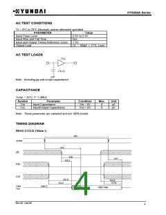
AC CHARACTERISTICS
Vcc = 5.0V±10%, TA = 0°C to 70°C (Normal), unless otherwise noted
-70
-85
-10
#
Parameter
Symbol
Unit
Min Max Min Max Min Max
READ CYCLE
1
tRC
Read Cycle Time
70
-
-
-
85
-
-
-
100
-
-
-
10
5
0
0
10
-
100
100
55
-
ns
ns
ns
ns
ns
ns
ns
ns
ns
2
3
4
5
6
7
8
9
tAA
Address Access Time
70
70
45
-
85
85
50
-
tACS
tOE
Chip Select Access Time
Output Enable to Output Valid
Chip Select to Output in Low Z
Output Enable to Outputin Low Z
Chip Deselection to Output in High Z
Out Disable to Output in High Z
Output Hold from Address Change
-
-
tCLZ
tOLZ
tCHZ
tOHZ
tOH
10
5
0
0
5
10
5
0
0
5
-
-
-
30
30
-
35
35
-
35
35
-
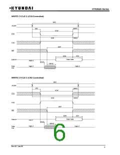
WRITE CYCLE
10 tWC
11 tCW
12 tAW
13 tAS
14 tWP
15 tWR
16 tWHZ
17 tDW
18 tDH
19 tOW
Write Cycle Time
70
55
55
0
50
0
0
35
0
-
-
-
-
-
-
30
-
-
-
85
60
60
0
55
0
0
35
0
-
-
-
-
-
-
35
-
-
-
100
70
70
0
60
0
0
40
0
-
-
-
-
-
-
35
-
-
-
ns
ns
ns
ns
ns
ns
ns
ns
ns
ns
Chip Selection to End of Write
Address Valid to End of Write
Address Set-up Time
Write Pulse Width
Write Recovery Time
Write to Output in High Z
Data to Write Time Overlap
Data Hold from Write Time
Output Active from End of Write
5
5
5
Rev.02 /Jan.99
3

 ETC [ ETC ]