HY6264A Series
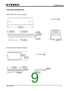
ORDERING INFORMATION
PART NO.
HY6264AP
HY6264ALP
HY6264ALLP
HY6264AJ
SPEED
70/85/100
70/85/100
70/85/100
70/85/100
70/85/100
70/85/100
POWER
L-part
PACKAGE
PDIP
PDIP
PDIP
SOP
SOP
SOP
LL-part
HY6264ALJ
HY6264ALLJ
L-part
LL-part
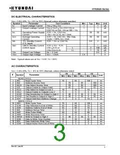
ABSOLUTE MAXIMUM RATING (1)
Symbol
Vcc, VIN, VOUT
TA
TSTG
PD
Parameter
Power Supply, Input/Output Voltage
Operating Temperature
Storage Temperature
Rating
-0.5 to 7.0
0 to 70
-65 to 125
1.0
Unit
V
°C
°C
W
Power Dissipation
IOUT
TSOLDER
Data Output Current
Lead Soldering Temperature & Time
50
260 ·10
mA
°C·sec
Note
1. Stresses greater than those listed under ABSOLUTE MAXIMUM RATINGS may cause permanent
damage to the device. This is stress rating only and the functional operation of the device under these
or any other conditions above those indicated in the operation of this specification is not implied.
Exposure to the absolute maximum rating conditions for an extended period may affect reliability.
RECOMMENDED DC OPERATING CONDITIONS
TA=0°C TO 70°C
Symbol
Vcc
VIH
Parameter
Min.
4.5
2.2
Typ.
5.0
-
-
Max.
5.5
Vcc+0.5
0.8
Unit
V
V
Supply Voltage
Input High Voltage
Input Low Voltage
VIL
-0.5(1)
V
Note
1.VIL = -3.0V for pulse width less than 50ns
TRUTH TABLE
/CS1
CS2
X
L
H
H
/WE
X
X
H
H
/OE
MODE
Standby
I/O OPERATION
High-Z
High-Z
High-Z
Data Out
Data In
H
X
L
L
L
X
X
H
L
Output Disabled
Read
Write
H
L
X
Note
1. H=VIH, L=VIL, X=Don't Care
Rev.02 /Jan.99
2

 ETC [ ETC ]