Freescale Semiconductor, Inc.
Hardware Design
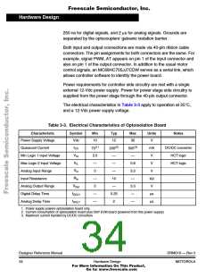
250 ns for digital signals, and 2 µs for analog signals. Grounds are
separated by the optocouplers’ galvanic isolation barrier.
Both input and output connections are made via 40-pin ribbon cable
connectors. The pin assignments for both connectors are the same. For
example, signal PWM_AT appears on pin 1 of the input connector and
also on pin 1 of the output connector. In addition to the usual motor
control signals, an MC68HC705JJ7CDW serves as a serial link, which
allows controller software to identify the power board.
Power requirements for controller side circuitry are met with a single
external 12-Vdc power supply. Power for power stage side circuitry is
supplied from the power stage through the 40-pin output connector.
The electrical characteristics in Table 3-3 apply to operation at 25°C,
and a 12-Vdc power supply voltage.
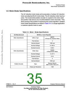
Table 3-3. Electrical Characteristics of Optoisolation Board
Characteristic
Power Supply Voltage
Quiescent Current
Symbol
Min
Typ
Max
Units
V
Notes
Vdc
10
12
30
(1)
(2)
(3)
I
mA
DC/DC converter
HCT logic
70
200
500
CC
V
Min Logic 1 Input Voltage
Max Logic 0 Input Voltage
Analog Input Range
Input Resistance
2.0
—
0
—
—
—
V
V
IH
V
0.8
3.3
—
HCT logic
IL
V
—
V
In
R
—
0
10
—
kΩ
V
In
V
Analog Output Range
Digital Delay Time
3.3
—
Out
t
—
—
0.25
2
µs
µs
DDLY
t
Analog Delay Time
—
ADLY
1. Power supply powers optoisolation board only.
2. Current consumption of optoisolation board plus DSP EVM board (powered from this power supply)
3. Maximum current handled by DC/DC converters
Designer Reference Manual
DRM019 — Rev 0
MOTOROLA
34
Hardware Design
For More Information On This Product,
Go to: www.freescale.com

 ETC [ ETC ]