Data Sheet
June 1999
ORCA Series 2 FPGAs
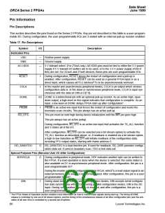
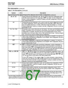
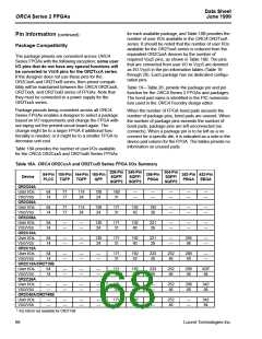
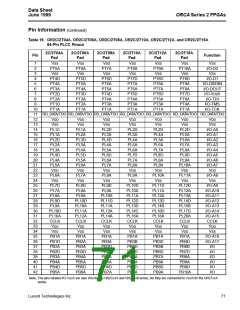
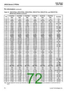
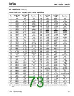
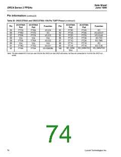
Pin Information (continued)
Compatibility with Series 3 FPGAs
Pinouts for the OR2CxxA, OR2TxxA, and OR2TxxB devices will be consistent with the Series 3 FPGAs for all
devices offered in the same packages. This includes the following pins: VDD, VSS, VDD5 (OR3C/Txxx series only),
and all configuration pins. Identical to the OR2TxxB devices, Series 3 devices provide 5 V tolerant I/Os without a
dedicated VDD5 supply
The following restrictions apply:
1. There are two configuration modes supported in the OR2C/TxxA series that are not supported in the
Series 3 FPGAs series: master parallel down and synchronous peripheral modes. The Series 3 FPGAs have two
new microprocessor interface (MPI) configuration modes that are unavailable in the Series 2.
2. There are 4 pins—one per each device side—that are user I/O in the OR2C/TxxA series which can only be used
as fast dedicated clocks or global inputs in the Series 3 series. These pins are also used to drive the Express-
CLK to the I/O FFs on their given side of the device. These four middle ExpressCLK pins should not be used to
connect to a programmable clock manager (PCM). A corner ExpressCLK input should be used instead (see note
below). See Table 18C for a list of these pins in each package.
3. There are two other pins that are user I/O in both the Series 2 and Series 3 series but also have optional added
functionality in the Series 3 series. Each of these pins drives the ExpressCLKs on two sides of the device. They
also have fast connectivity to the programmable clock manager (PCM). See Table 18C for a preliminary list of
these pins in each package.
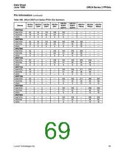
Table 18C. Series 3 ExpressCLK Pins
Pin Name/
Package
208-Pin
SQFP2
240-Pin
SQFP2
256-Pin
PBGA
352-Pin
PBGA
432-Pin
EBGA
600-Pin
EBGA
ECKL
ECKB
22
80
26
91
K3
W11
K18
B11
W1
N2
AE14
N23
B14
AB4
A25
R29
AH16
T2
U33
AM18
V2
ECKR
131
178
49
152
207
56
ECKT
C15
AG29
D5
C17
AK34
D5
I/O—SECKLL
I/O—SECKUR
159
184
A19
Note: The ECKR, ECKL, ECKT, and ECKB pins drive the ExpressCLK on their given edge of the device, while I/O—SECKLL and
I/O—SECKUR drive an ExpressCLK on two edges of the device and provide connectivity to the programmable clock manager.
70
Lucent Technologies Inc.

 ETC [ ETC ]