Data Sheet
June 1999
ORCA Series 2 FPGAs
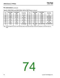
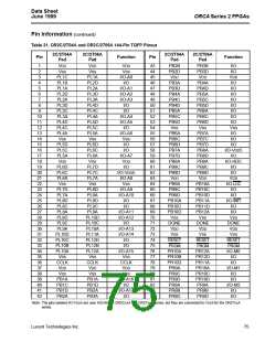
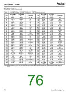
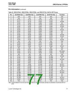
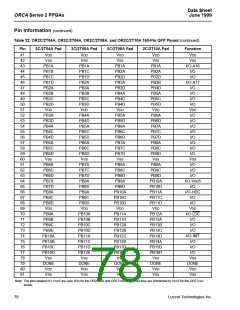
Pin Information (continued)
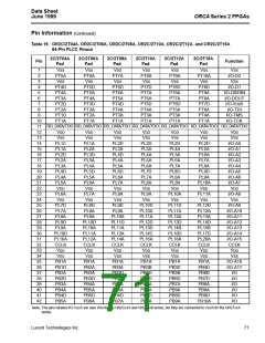
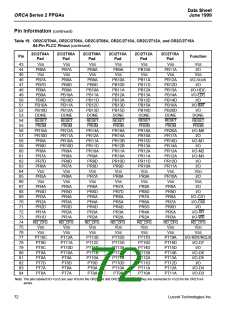
Table 20. OR2C/2T04A and OR2C/2T06A 100-Pin TQFP Pinout (continued)
2C/2T04A
Pad
2C/2T06A
Pad
2C/2T04A
Pad
2C/2T06A
Pad
Pin
Function
Pin
Function
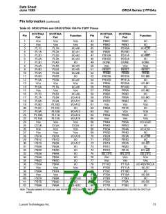
85
86
87
88
89
90
91
92
PT7A
PT6D
PT6A
VSS
PT5A
VSS
PT8A
PT7D
PT7A
VSS
PT6A
VSS
I/O-D4
I/O
I/O-D3
VSS
I/O-D2
VSS
93
94
95
96
97
98
99
100
PT3D
PT3A
PT2D
PT2A
PT1D
PT1C
PT1A
RD_DATA/
TDO
PT4D
PT4A
PT3D
PT3A
PT2A
I/O
I/O-DOUT
I/O-VDD5
I/O-TDI
I/O-TMS
I/O
PT1D
PT1A
PT4D
PT4A
PT5D
PT5A
I/O-D1
I/O-D0/DIN
I/O-TCK
RD_DATA/TDO
RD_DATA/TDO
Note: The pins labeled I/O-VDD5 are user I/Os for the OR2CxxA and OR2TxxB series, but they are connected to VDD5 for the OR2TxxA
series.
74
Lucent Technologies Inc.

 ETC [ ETC ]