Data Sheet
June 1999
ORCA Series 2 FPGAs
Pin Information (continued)
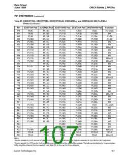
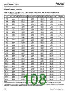
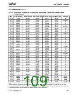
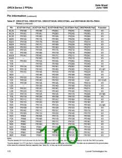
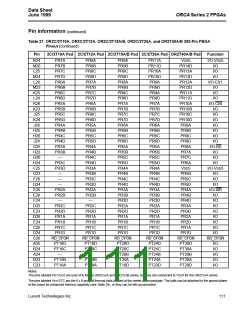
Table 27. OR2C/2T10A, OR2C/2T12A, OR2C/2T15A/B, OR2C/2T26A, and OR2T40A/B 352-Pin PBGA
Pinout (continued)
Pin
2C/2T10A Pad 2C/2T12A Pad 2C/2T15A/B Pad 2C/2T26A Pad OR2T40A/B Pad
Function
P4
P1
PL9C
PL9B
PL9A
PL10D
PL10C
PL10B
PL10A
PL11D
PL11C
PL11B
PL11A
PL12D
—
PL10C
PL10B
PL10A
PL11D
PL11C
PL11B
PL11A
PL12D
PL12C
PL12B
PL12A
PL13D
PL13C
PL13B
PL13A
PL14D
PL14C
PL14B
PL14A
PL15D
PL15C
PL15B
PL15A
PL16D
PL16C
PL16B
PL16A
PL17D
PL17C
PL17B
PL17A
PL18D
PL18C
PL18B
—
PL11C
PL11B
PL11A
PL12D
PL12C
PL12B
PL12A
PL13D
PL13C
PL13B
PL13A
PL14D
PL14C
PL14B
PL14A
PL15D
PL15C
PL15B
PL15A
PL16D
PL16C
PL16B
PL16A
PL17D
PL17C
PL17B
PL17A
PL18D
PL18C
PL18A
PL19D
PL19C
PL19A
PL20D
PL20C
PL20B
PL20A
CCLK
PL13C
PL13B
PL13A
PL14D
PL14A
PL15D
PL15A
PL16D
PL16A
PL17D
PL17A
PL18D
PL18C
PL18B
PL18A
PL19D
PL19C
PL19B
PL19A
PL20D
PL20C
PL20B
PL20A
PL21D
PL21C
PL21B
PL21A
PL22D
PL22C
PL22A
PL23D
PL23C
PL23A
PL24D
PL24C
PL24B
PL24A
CCLK
VDD5
PL16B
PL16A
PL17D
PL17A
PL18D
PL18A
PL19D
PL19A
PL20D
PL20A
PL21D
PL21C
PL21B
PL21A
PL22D
PL22C
PL22B
PL22A
PL23D
PL23C
PL24D
PL25D
PL25A
PL26C
PL26B
PL26A
VDD5
I/O-VDD5
I/O
N3
I/O-A8
I/O-A9
I/O
R2
P3
R1
I/O
T2
I/O-A10
I/O
R3
T1
I/O
R4
I/O
U2
I/O-A11
I/O-A12
I/O
T3
U1
U4
PL12C
—
I/O
V2
I/O
U3
PL12B
PL12A
PL13D
PL13C
PL13B
PL13A
PL14D
—
I/O
V1
I/O
W2
W1
V3
I/O-A13
I/O
I/O
Y2
I/O
W4
Y1
I/O
I/O
W3
AA2
Y4
PL14C
PL14B
PL14A
—
I/O-A14
I/O
I/O
AA1
Y3
I/O
PL15D
PL15C
PL15B
PL15A
PL16D
PL16C
PL16B
—
I/O-VDD5
I/O
AB2
AB1
AA3
AC2
AB4
AC1
AB3
AD2
AC3
AD1
AF2
PL27C
PL27A
PL28D
PL28C
PL28A
PL29A
PL30C
PL30B
PL30A
PCCLK
PB1A
I/O
I/O
I/O
I/O
I/O
I/O
—
—
I/O
PL16A
CCLK
PB1A
PL18A
CCLK
PB1A
I/O-A15
CCLK
I/O-A16
PB1A
PB1A
Notes:
The pins labeled I/O-VDD5 are user I/Os for the OR2CxxA and OR2TxxB series, but they are connected to VDD5 for the OR2TxxA series.
The pins labeled VSS-ETC are the 6 x 6 array of thermal balls located at the center of the package. The balls can be attached to the ground plane
of the board for enhanced thermal capability (see Table 29), or they can be left unconnected.
Lucent Technologies Inc.
107

 ETC [ ETC ]