Data Sheet
June 1999
ORCA Series 2 FPGAs
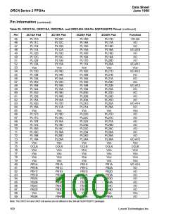
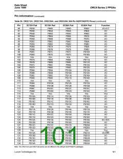
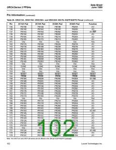
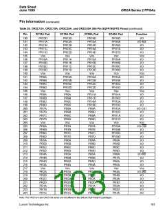
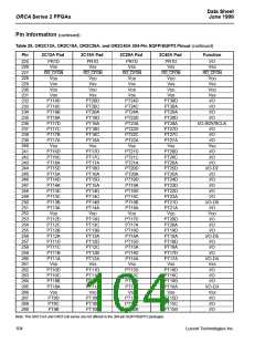
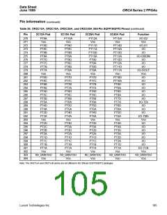
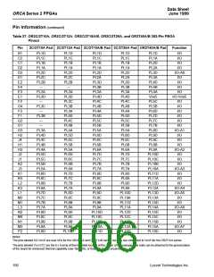
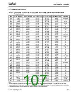
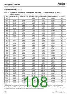
Pin Information (continued)
Table 26. OR2C12A, OR2C15A, OR2C26A, and OR2C40A 304-Pin SQFP/SQFP2 Pinout (continued)
Pin
2C12A Pad
2C15A Pad
2C26A Pad
2C40A Pad
Function
225
226
227
228
229
230
231
232
233
234
235
236
237
238
239
240
241
242
243
244
245
246
247
248
249
250
251
252
253
254
255
256
257
258
259
260
261
262
263
264
265
266
267
268
269
PR1D
VSS
RD_CFGN
VDD
PR1D
VSS
RD_CFGN
VDD
PR1D
VSS
RD_CFGN
VDD
PR1D
VSS
RD_CFGN
VDD
I/O
VSS
RD_CFGN
VDD
VSS
VDD
VSS
I/O
VSS
VDD
VSS
VSS
VDD
VSS
VSS
VDD
VSS
VSS
VDD
VSS
PT18D
PT18C
PT18B
PT18A
PT17D
PT17C
PT17B
PT17A
VSS
PT16D
PT16C
PT16A
PT15D
PT15A
PT14D
PT14A
PT13D
PT13C
PT13B
PT13A
VDD
PT12D
PT12C
PT12B
PT12A
PT11D
PT11C
PT11B
PT11A
VSS
PT10D
PT10C
PT10B
PT10A
VSS
PT20D
PT20C
PT20A
PT19D
PT19A
PT18D
PT18C
PT18A
VSS
PT17D
PT17C
PT17A
PT16D
PT16A
PT15D
PT15A
PT14D
PT14C
PT14B
PT14A
VDD
PT13D
PT13C
PT13B
PT13A
PT12D
PT12C
PT12B
PT12A
VSS
PT11D
PT11C
PT11B
PT11A
VSS
PT24D
PT24C
PT24A
PT23D
PT23A
PT22D
PT22C
PT22A
VSS
PT21D
PT21C
PT21A
PT20D
PT20A
PT19D
PT19A
PT18D
PT18C
PT18B
PT18A
VDD
PT17D
PT17A
PT16D
PT16A
PT15D
PT15A
PT14D
PT14A
VSS
PT13D
PT13C
PT13B
PT13A
VSS
PT30D
PT30A
PT29A
PT28D
PT28A
PT27D
PT27C
PT27A
VSS
PT26D
PT26C
PT26A
PT25D
PT25A
PT24D
PT23D
PT22D
PT22A
PT21D
PT21A
VDD
PT20D
PT20A
PT19D
PT19A
PT18D
PT18A
PT17D
PT17A
VSS
PT16D
PT16C
PT16B
PT16A
VSS
I/O
I/O
I/O
I/O-RDY/RCLK
I/O
I/O
I/O
VSS
I/O
I/O
I/O
I/O-D7
I/O
I/O
I/O
I/O
I/O
I/O-D6
I/O
VDD
I/O
I/O
I/O
I/O-D5
I/O
I/O
I/O
I/O-D4
VSS
I/O
I/O
I/O
I/O-D3
VSS
I/O
I/O
I/O
PT9D
PT9C
PT9B
PT10D
PT10C
PT10B
PT12D
PT12C
PT12B
PT15D
PT15C
PT15B
Note: The OR2TxxA and OR2TxxB series are not offered in the 304-pin SQFP/SQFP2 packages.
104
Lucent Technologies Inc.

 ETC [ ETC ]