Data Sheet
June 1999
ORCA Series 2 FPGAs
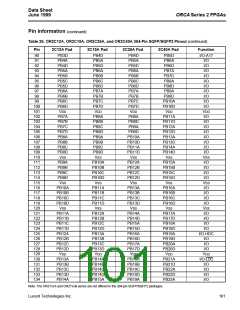
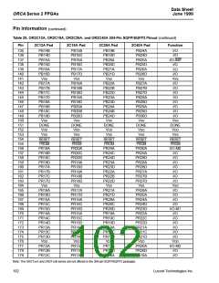
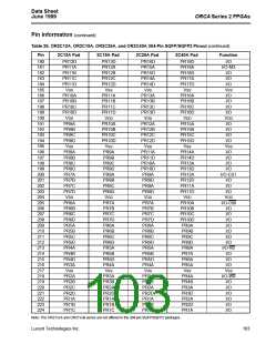
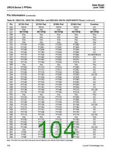
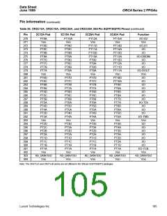
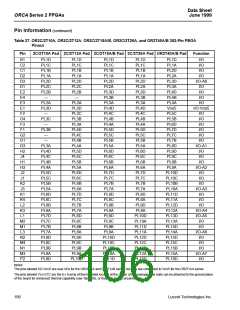
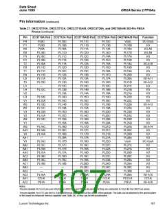
Pin Information (continued)
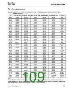
Table 26. OR2C12A, OR2C15A, OR2C26A, and OR2C40A 304-Pin SQFP/SQFP2 Pinout (continued)
Pin
2C12A Pad
2C15A Pad
2C26A Pad
2C40A Pad
Function
270
271
272
273
274
275
276
277
278
279
280
281
282
283
284
285
286
287
288
289
290
291
292
293
294
295
296
297
298
299
300
301
302
303
304
PT9A
VSS
PT10A
VSS
PT12A
VSS
PT15A
VSS
I/O-D2
VSS
I/O-D1
I/O
I/O
I/O-D0/DIN
I/O
I/O
I/O
I/O-DOUT
VDD
I/O
I/O
I/O
I/O
I/O
I/O
I/O
I/O-TDI
I/O
PT8D
PT8C
PT8B
PT8A
PT7D
PT7C
PT7B
PT7A
VDD
PT6D
PT6C
PT6B
PT6A
PT5D
PT5C
PT5B
PT5A
PT4D
PT4A
PT3D
PT3A
VSS
PT2D
PT2C
PT2B
PT2A
PT1D
PT1C
PT1B
PT1A
VSS
PT9D
PT9C
PT9B
PT9A
PT8D
PT8C
PT8B
PT8A
VDD
PT7D
PT7C
PT7B
PT7A
PT6D
PT6C
PT6B
PT6A
PT5D
PT5A
PT4D
PT4A
VSS
PT3D
PT3A
PT2D
PT2A
PT1D
PT1C
PT1B
PT1A
VSS
PT11D
PT11A
PT10D
PT10A
PT9D
PT9A
PT8D
PT8A
VDD
PT7D
PT7C
PT7B
PT7A
PT6D
PT6C
PT6B
PT6A
PT5D
PT5A
PT4D
PT4A
VSS
PT3D
PT3A
PT2D
PT2A
PT1D
PT1C
PT1B
PT1A
VSS
PT14D
PT14A
PT13D
PT13A
PT12D
PT12A
PT11D
PT11A
VDD
PT10D
PT10A
PT9D
PT9A
PT8D
PT8A
PT7D
PT7A
PT6D
PT6A
PT5D
PT5A
VSS
PT4D
PT4A
PT3D
PT3A
PT2D
PT2A
PT1D
PT1A
VSS
I/O
I/O
I/O-TMS
VSS
I/O
I/O
I/O
I/O
I/O
I/O
I/O
I/O-TCK
VSS
RD_DATA/TDO
RD_DATA/TDO
RD_DATA/TDO
VDD
RD_DATA/TDO
VDD
RD_DATA/TDO
VDD
VDD
VDD
Note: The OR2TxxA and OR2TxxB series are not offered in the 304-pin SQFP/SQFP2 packages.
Lucent Technologies Inc.
105

 ETC [ ETC ]