Data Sheet
June 1999
ORCA Series 2 FPGAs
Timing Characteristics (continued)
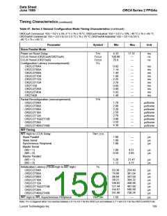
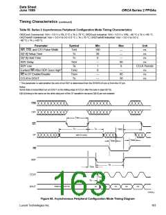
Table 50. Series 2 Asynchronous Peripheral Configuration Mode Timing Characteristics
OR2CxxA Commercial: VDD = 5.0 V ± 5%, 0 °C ≤ TA ≤ 70 °C; OR2CxxA Industrial: VDD = 5.0 V ± 10%, –40 °C ≤ TA ≤ +85 °C.
OR2TxxA/B Commercial: VDD = 3.0 V to 3.6 V, 0 °C ≤ TA ≤ 70 °C; OR2TxxA/B Industrial: VDD = 3.0 V to 3.6 V,
–40 °C ≤ TA ≤ +85 °C.
Parameter
WR, CS0, and CS1 Pulse Width
D[7:0] Setup Time
Symbol
TWR
TS
Min
100
20
0
Max
—
—
—
60
8
Unit
ns
ns
D[7:0] Hold Time
TH
ns
RDY Delay
TRDY
TB
—
1
ns
RDY Low
CCLK Periods
Earliest WR After RDY Goes High*
RD to D7 Enable/Disable
CCLK to DOUT
TWR2
TDEN
TD
0
—
60
30
ns
ns
ns
—
—
* This parameter is valid whether the end of not RDY is determined from the RDY/RCLK pin or from the D7 pin.
Notes:
Serial data is transmitted out on DOUT on the falling edge of CCLK after the byte is input D[7:0].
D[6:0] timing is the same as the write data port of the D7 waveform because D[6:0] are not enabled.
CS0
CS1
TWR
WR
TS
TH
TWR2
D7
WRITE DATA
TDEN
TDEN
RD
RDY
TB
TRDY
CCLK
DOUT
TD
D0
D1
D2
D3
PREVIOUS BYTE
D7
5-4533.a
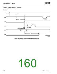
Figure 68. Asynchronous Peripheral Configuration Mode Timing Diagram
Lucent Technologies Inc.
163

 ETC [ ETC ]