Data Sheet
June 1999
ORCA Series 2 FPGAs
Timing Characteristics (continued)
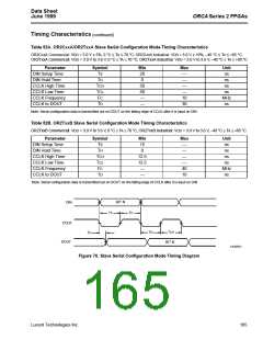
Table 53A. OR2CxxA/OR2TxxA Slave Parallel Configuration Mode Timing Characteristics
OR2CxxA Commercial: VDD = 5.0 V ± 5%, 0 °C ≤ TA ≤ 70 °C; OR2CxxA Industrial: VDD = 5.0 V ± 10%, –40 °C ≤ TA ≤ +85 °C.
OR2TxxA Commercial: VDD = 3.0 V to 3.6 V, 0 °C ≤ TA ≤ 70 °C; OR2TxxA Industrial: VDD = 3.0 V to 3.6 V, –40 °C ≤ TA ≤ +85 °C.
Parameter
CS0, CS1, WR Setup Time
CS0, CS1, WR Hold Time
D[7:0] Setup Time
D[7:0] Hold Time
Symbol
TS1
Min
60
20
20
0
Max
—
Unit
ns
TH1
—
ns
TS2
—
ns
TH2
—
ns
CCLK High Time
TCH
TCL
50
50
—
—
ns
CCLK Low Time
—
ns
CCLK Frequency
FC
10
MHz
Note: Daisy chaining of FPGAs is not supported in this mode.
Table 53B. OR2TxxB Slave Parallel Configuration Mode Timing Characteristics
OR2TxxB Commercial: VDD = 3.0 V to 3.6 V, 0 °C ≤ TA ≤ 70 °C; OR2TxxB Industrial: VDD = 3.0 V to 3.6 V, –40 °C ≤ TA ≤ +85 °C.
Parameter
CS0, CS1, WR Setup Time
CS0, CS1, WR Hold Time
D[7:0] Setup Time
D[7:0] Hold Time
Symbol
TS1
Min
—
Max
—
Unit
—
TH1
15
—
ns
TS2
15
—
ns
TH2
0
—
ns
CCLK High Time
TCH
TCL
12.5
12.5
—
—
ns
CCLK Low Time
—
ns
CCLK Frequency
FC
40
MHz
Note: Daisy chaining of FPGAs is not supported in this mode.
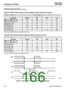
CS0
CS1
WR
TS1
H1
T
CCLK
TH2
TS2
D[7:0]
5-2848(F)
Figure 71. Slave Parallel Configuration Mode Timing Diagram
166
Lucent Technologies Inc.

 ETC [ ETC ]