Data Sheet
June 1999
ORCA Series 2 FPGAs
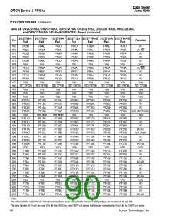
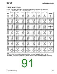
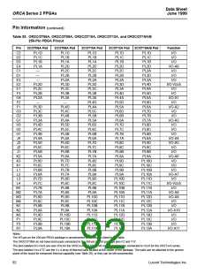
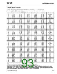
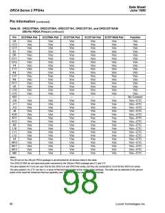
Pin Information (continued)
Table 25. OR2C/2T06A, OR2C/2T08A, OR2C/2T10A, OR2C/2T12A, and OR2C/2T15A/B
256-Pin PBGA Pinout (continued)
Pin
Function
2C/2T06A Pad
PB6A
PB6B
PB6C
PB6D
PB7A
PB7B
PB7C
PB7D
PB8A
PB8B
PB8C
PB8D
PB9A
PB9B
PB9C
PB9D
PB10A
PB10B
PB10C
PB10D
—
2C/2T08A Pad
PB7A
2C/2T10A Pad
PB8A
2C/2T12A Pad
PB9A
2C/2T15A/B Pad
PB10A
PB10B
PB10C
PB10D
PB11A
PB11B
PB11C
PB11D
PB12A
PB12B
PB12C
PB12D
PB13A
PB13B
PB13C
PB13D
PB14A
PB14B
PB14C
PB14D
PB15A
PB15D
PB16A
PB16D
PB17A
PB17D
PB18A
PB18D
PB19A
PB19D
PB20A
PB20B
PB20D
DONE
W10
V10
Y10
Y11
W11
V11
U11
Y12
W12
V12
U12
Y13
W13
V13
Y14
W14
Y15
V14
W15
Y16
U14
V15
W16
Y17
V16
W17
Y18
U16
V17
W18
Y19
V18
W19
Y20
W20
V19
U19
U18
T17
V20
I/O
I/O
I/O
I/O
I/O
I/O
I/O
I/O
PB7B
PB7C
PB7D
PB8A
PB8B
PB8C
PB8D
PB9A
PB8B
PB8C
PB8D
PB9A
PB9B
PB9C
PB9D
PB9B
PB9C
PB9D
PB10A
PB10B
PB10C
PB10D
PB11A
PB11B
PB11C
PB11D
PB12A
PB12B
PB12C
PB12D
PB13A
PB13B
PB13C
PB13D
PB14A
PB14D
PB15A
PB15D
PB16A
PB16D
PB17A
PB17C
PB17D
PB18A
PB18B
PB18C
PB18D
DONE
RESET
PRGM
PB10A
PB10B
PB10C
PB10D
PB11A
PB11B
PB11C
PB11D
PB12A
PB12C
PB12D
PB13A
PB13B
PB13C
PB13D
PB14A
PB14B
PB15A
PB15B
PB15C
PB15D
PB16A
PB16B
PB16C
PB16D
DONE
RESET
PRGM
I/O-VDD5
I/O
I/O
I/O
I/O-HDC
I/O
I/O
I/O
I/O-LDC
I/O
PB9B
PB9C
PB9D
PB10A
PB10B
PB10C
PB10D
PB11A
PB11B
PB11C
PB11D
PB12A
PB12B
PB12C
—
PB12D
PB13A
PB13B
PB13C
PB13D
PB14A
PB14B
PB14C
PB14D
DONE
RESET
PRGM
I/O
I/O
I/O
I/O
—
PB11A
—
I/O-INIT
I/O
I/O-VDD5
I/O
—
PB11B
PB11C
PB11D
PB12A
PB12B
PB12C
PB12D
—
DONE
RESET
PRGM
PR12A
—
I/O
I/O
I/O
I/O
I/O
I/O
I/O
DONE
RESET
PRGM
I/O-M0
I/O
RESET
PRGM
PR14A
PR14C
PR14D
PR13A
PR16A
PR16C
PR16D
PR15A
PR18A
PR18C
PR18D
PR17A
PR20A
PR20D
PR19A
PR19D
—
—
I/O
I/O
Notes:
The W3 pin on the 256-pin PBGA package is unconnected for all devices listed in this table.
The OR2C/2T08A do not have bond pads connected to the 256-pin PBGA package pins F2 and Y17.
The pins labeled I/O-VDD5 are user I/Os for the OR2CxxA and OR2TxxB series, but they are connected to VDD5 for the OR2TxxA series.
The pins labeled VSS-ETC are the 4 x 4 array of thermal balls located at the center of the package. The balls can be attached to the ground
plane of the board for enhanced thermal capability (see Table 29), or they can be left unconnected.
94
Lucent Technologies Inc.

 ETC [ ETC ]