Data Sheet
June 1999
ORCA Series 2 FPGAs
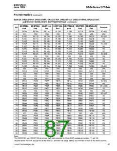
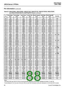
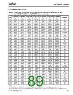
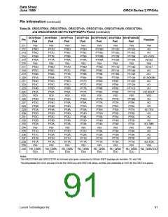
Pin Information (continued)
Table 24. OR2C/2T06A, OR2C/2T08A, OR2C/2T10A, OR2C/2T12A, OR2C/2T15A/B, OR2C/2T26A,
and OR2C/2T40A/B 240-Pin SQFP/SQFP2 Pinout (continued)
2C/2T06A 2C/2T08A 2C/2T10A 2C/2T12A 2C/2T15A/B 2C/2T26A 2C/2T40A/B
Pin
Function
Pad
Pad
Pad
Pad
Pad
Pad
Pad
211
212
213
214
215
216
217
218
219
220
221
222
223
224
225
226
227
228
229
230
231
232
233
234
235
236
237
238
239
240
VSS
VSS
VSS
PT8D
PT8C
PT8B
PT8A
VSS
VSS
PT9D
PT9C
PT9B
PT9A
VSS
VSS
PT10D
PT10C
PT10B
PT10A
VSS
VSS
PT12D
PT12C
PT12B
PT12A
VSS
VSS
PT15D
PT15C
PT15B
PT15A
VSS
VSS
I/O
PT6D
PT6C
PT6B
PT6A
VSS
PT7D
PT7C
PT7B
PT7A
VSS
I/O
I/O-VDD5
I/O-D2
VSS
PT5D
PT5C
PT5B
PT5A
PT4D
PT4C
PT4B
PT4A
VDD
PT6D
PT6C
PT6B
PT6A
PT5D
PT5C
PT5B
PT5A
VDD
PT7D
PT7C
PT7B
PT7A
PT6D
PT6C
PT6B
PT6A
VDD
PT8D
PT8C
PT8B
PT8A
PT7D
PT7C
PT7B
PT7A
VDD
PT9D
PT9C
PT9B
PT9A
PT8D
PT8C
PT8B
PT8A
VDD
PT11D
PT11A
PT10D
PT10A
PT9D
PT9A
PT8D
PT8A
VDD
PT14D
PT14A
PT13D
PT13A
PT12D
PT12A
PT11D
PT11A
VDD
I/O-D1
I/O
I/O
I/O-D0/DIN
I/O
I/O
I/O
I/O-DOUT
VDD
PT3D
PT3C
PT3B
PT3A
PT2D
PT2C
PT2B
PT2A
VSS
PT4D
PT4C
PT4B
PT4A
PT3D
PT3C
PT3B
PT3A
VSS
PT5D
PT5A
PT4D
PT4A
PT3D
PT3C
PT3B
PT3A
VSS
PT6D
PT6A
PT5C
PT5A
PT4D
PT4A
PT3D
PT3A
VSS
PT7D
PT7A
PT6C
PT6A
PT5D
PT5A
PT4D
PT4A
VSS
PT7D
PT7A
PT6C
PT6A
PT5D
PT5A
PT4D
PT4A
VSS
PT10D
PT9A
PT8A
PT7A
PT6D
PT6A
PT5D
PT5A
VSS
I/O
I/O
I/O
I/O-TDI
I/O
I/O
I/O
I/O-TMS
VSS
PT1D
PT1C
PT1B
PT1A
VSS
PT2D
PT2A
PT1D
PT1A
VSS
PT2D
PT2A
PT1D
PT1A
VSS
PT2C
PT2A
PT1D
PT1A
VSS
PT3A
PT2A
PT1D
PT1A
VSS
PT3A
PT2A
PT1D
PT1A
VSS
PT4A
PT3A
PT2D
PT1A
VSS
I/O
I/O
I/O
I/O-TCK
VSS
RD_DATA/
TDO
RD_DATA/
TDO
RD_DATA/
TDO
RD_DATA/
TDO
RD_DATA/
TDO
RD_DATA/
TDO
RD_DATA/ RD_DATA/TDO
TDO
Notes:
The OR2C/2T08A and OR2C/2T10A do not have bond pads connected to 240-pin SQFP package pin numbers 113 and 188.
The pins labeled I/O-VDD5 are user I/Os for the OR2CxxA and OR2TxxB series, but they are connected to VDD5 for the OR2TxxA series.
Lucent Technologies Inc.
91

 ETC [ ETC ]