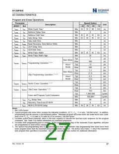
HY29F800
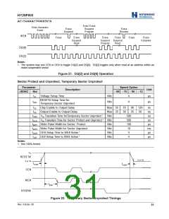
AC CHARACTERISTICS
Program and Erase Operations
Parameter
Speed Option
Description
Unit
JEDEC
tAVAV
Std
- 55 - 70 - 90 - 12
tWC Write Cycle Time 1
Min 55
Min
70
90
120
ns
ns
tAVWL
tAS
Address Setup Time
0
tWLAX
tDVWH
tWHDX
tGHWL
tELWL
tAH Address Hold Time
tDS Data Setup Time
tDH Data Hold Time
Min 45
Min 25
Min
45
30
45
45
50
50
ns
ns
0
0
0
0
ns
tGHWL Read Recovery Time Before Write
tCS CE# Setup Time
Min
ns
Min
ns
tWHEH
tWLWH
tWHWL
tCH CE# Hold Time
Min
ns
tWP Write Pulse Width
Min 30
Min
35
45
50
ns
tWPH Write Pulse Width High
20
7
ns
Typ
µs
Byte Mode
Max
300
12
µs
tWHWH1 tWHWH1 Programming Operation 1, 2, 3
Typ
µs
Word
Mode
Max
500
7.2
21.6
6.3
18.6
1
µs
Typ
sec
sec
sec
sec
sec
sec
sec
sec
cycles
cycles
µs
Byte Mode
Max
Chip Programming Operation 1, 2, 3, 5
Typ
Word
Mode
Max
Typ
tWHWH2 tWHWH2 Sector Erase Operation 1, 2, 4
tWHWH3 tWHWH3 Chip Erase Operation 1, 2, 4
Erase and Program Cycle Endurance
Max
8
Typ
19
Max
150
Typ
1,000,000
Min
100,000
tVCS VCC Setup Time
Min
50
0
tRB Recovery Time from RY/BY#
tBUSY WE# to RY/BY# Delay
Min
ns
Min 30
30
35
50
ns
Notes:
1. Not 100% tested.
2. Typical program and erase times assume the following conditions: 25 °C, VCC = 5.0 volts, 100,000 cycles. In addition,
programming typicals assume a checkerboard pattern. Maximum program and erase times are under worst case condi-
tions of 90 °C, VCC = 4.5 volts (4.75 volts for 55 ns version), 100,000 cycles.
3. Excludes system-level overhead, which is the time required to execute the four-bus-cycle sequence for the program
command. See Table 5 for further information on command sequences.
4. Excludes 0x00 programming prior to erasure. In the preprogramming step of the Automatic Erase algorithm, all bytes
are programmed to 0x00 before erasure.
5. The typical chip programming time is considerably less than the maximum chip programming time listed since most
bytes program faster than the maximum programming times specified. The device sets DQ[5] = 1 only If the maximum
byte program time specified is exceeded. See Write Operation Status section for additional information.
Rev. 4.0/Jan. 00
27

 ETC [ ETC ]