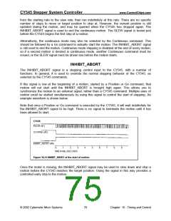
CY545 Stepper System Controller
www.ControlChips.com
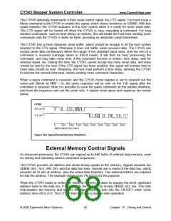
The CY545 provides all address and strobe timing signals to the display. Signals required are
HP_SEL (shared function with USRB7), ALE, WR, RD, and the data bus lines. For the HP
display, only the lower 6 address signals are used, and they are generated from the data bus
and ALE signals. The address signals must be demultiplexed by an external latch, such as the
74LS373. If external memory is also being used in the system, the same address latch used for
the lower byte of the memory address may be connected to the display. This is shown in the
example schematic.
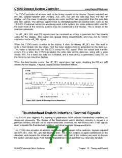
The HP _SEL, RD, and WR signals must be combined as shown to generate the Chip Enable
signal for the display. This signal has special timing requirements, and may not be simply
connected to the HP_SEL signal.
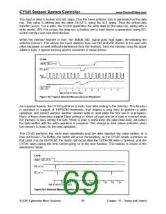
When the CY545 reads or writes to the display, it starts by driving HP_SEL low. The read or
write is then broken into two steps. First the lower address byte is generated on the data bus.
This value is latched into the 74LS373, using the ALE signal. Then the actual data transfer
occurs. For a write, the CY545 generates the write data on the data bus, along with a write
strobe, WR. For a read, the data bus is floated, and a read strobe is generated, using RD, so
the memory can now drive the bus.
When the data transfer is over, the HP_SEL signal goes high again, disabling the RD and WR
strobes for the display. A typical display access waveform follows.
Thumbwheel Switch Interface Control Signals
The CY545 also supports the reading of parameters from external thumbwheel switches, as
discussed previously. The design of the thumbwheel switch interface circuitry is shown in a
previous section, and will not be reproduced here. However, we will discuss the CY545 signals
used to enable the thumbwheel switches, and show example timing waveforms.
The CY545 also provides all address and strobe timing signals to the switches. Signals required
are SW_SEL, ALE, RD, and the data bus lines. The switch address is again multiplexed on the
data bus, and requires the external address latch. All 8 bits of the address are used to decode
the switch selection logic. Note that the thumbwheel switch interface is a read-only function.
© 2002 Cybernetic Micro Systems
66
Chapter 16 - Timing and Control

 ETC [ ETC ]