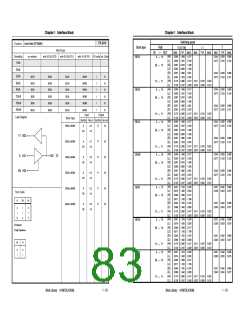
Chapter 1 Interface Block
Input Buffer with EN(OR)
Chapter 1 Interface Block
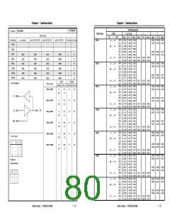
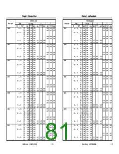
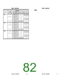
Switching speed
t LD0 (ns)
5.0 V
Function
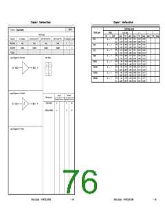
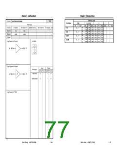
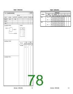
Block type
FN14
Path
→
t 1
T
Block type
with 50 KΩ P/U
IN
OUT
MIN.
0.103
0.223
0.164
0.203
0.103
0.223
0.164
0.203
TYP. MAX. MIN.
TYP. MAX. MIN.
TYP. MAX.
Function
Normal
Schmitt
Clock
no resistor
FN14
with 50 KΩ P/D
with 5 KΩ P/U
I/O cells int. Cells
(HH)
(LL)
(HH)
(LL)
(HH)
(LL)
(HH)
(LL)
0.166
0.311
0.241
0.331
0.166
0.311
0.241
0.331
0.247
0.432
0.365
0.596
0.247
0.432
0.365
0.596
0.011
0.007
0.011
0.007
0.011
0.007
0.011
0.007
0.015
0.009
0.015
0.009
0.015
0.009
0.015
0.009
0.021
0.013
0.022
0.013
0.021
0.013
0.022
0.013
A
→
→
→
→
Y
Y
Y
Y
FN24
1
4
EN
A
FN24
EN
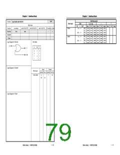
Logic Diagram for "Normal"
H01
Truth Table
A
A
EN
Y
N01
Y
0
0
1
1
0
1
0
1
0
1
1
1
H02 EN
Logic Diagram for "Schmitt"
Input
Output
Block type
FN14 to FN24
Symbol Fan-In Symbol Fan-Out
A
-
Y
34
EN
2.0
Logic Diagram for "Clock"
Block Library A13872EJ5V0BL
1 - 70
Block Library A13872EJ5V0BL
1 - 71

 ETC [ ETC ]