Proprietary TranSwitch Corporation Information for use Solely by its Customers
L3M
TXC-03452B
DATA SHEET
LIST OF FIGURES
Figure
Page
1.
2.
3.
4.
5.
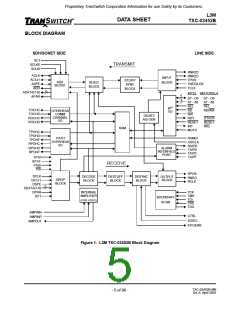
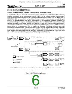
L3M TXC-03452B Block Diagram .......................................................... 5
L3M Multiplexing Structure ..................................................................... 6
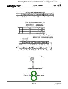
ITU-TSS TUG-3 Build Format ................................................................ 8
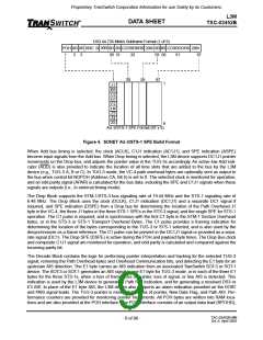
SONET AU-3/STS-1 SPE Build Format ................................................. 9
Lead Diagram for L3M TXC-03452B 144-Lead Plastic
Quad Flat Package .............................................................................. 11
Lead Diagram foe L3M TXC-03452B 208-Lead Plastic
6.
Ball Grid Array Package ....................................................................... 12
Line Side Transmit Timing ................................................................... 27
Line Side Receive Timing .................................................................... 28
STM-1 Add Bus Derived Interface Timing ............................................ 29
STS-3 Add Bus Derived Interface Timing ............................................ 30
STS-1 Add Bus Derived Interface Timing ............................................ 31
STM-1 Drop Bus Interface Timing ........................................................ 32
STS-3 Drop Bus Interface Timing ........................................................ 33
STS-1 Drop Bus Interface Timing ........................................................ 34
STS-1 Add Bus Interface Timing Using an External Clock .................. 35
STM-1 Add/Drop Bus Interface Timing ................................................ 36
STS-3 Add/Drop Bus Interface Timing ................................................. 37
STS-1 Add/Drop Bus Interface Timing ................................................. 38
Transmit Path Overhead Timing .......................................................... 39
Receive Path Overhead Timing ........................................................... 40
Transmit Alarm Indication Port Timing ................................................. 41
Receive Alarm Indication Port Timing .................................................. 42
Transmit Overhead Communications Channel Timing ........................ 42
Receive Overhead Communications Channel Interface Timing .......... 43
Intel Microprocessor Read Cycle Timing ............................................. 44
Intel Microprocessor Write Cycle Timing .............................................. 45
Motorola Microprocessor Read Cycle Timing ...................................... 46
Motorola Microprocessor Write Cycle Timing ...................................... 47
Boundary Scan Timing ......................................................................... 48
L3M Power-Up Reset Sequence .......................................................... 49
Physical Design For Analog Power Distribution ................................... 50
PLL Connection to External VCXO ...................................................... 51
Jitter Results for STS-3/DS3 and TUG-3/E3 Mappings ....................... 52
Loopbacks, Test Generators and Analyzer .......................................... 54
External Circuit to Maintain Clock Input to TX PRBS Generator .......... 54
Boundary Scan Schematic ................................................................... 56
L3M TXC-03452B 144-Lead Plastic Quad Flat Package ..................... 86
L3M TXC-03452B 208-Lead Small Outline
7.
8.
9.
10.
11.
12.
13.
14.
15.
16.
17.
18.
19.
20.
21.
22.
23.
24.
25.
26.
27.
28.
29.
30.
31.
32.
33.
34.
35.
36.
37.
38.
Plastic Ball Grid Array Package ........................................................... 87
TXC-03452B-MB
Ed. 6, April 2001
- 3 of 96 -

 ETC [ ETC ]