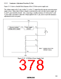
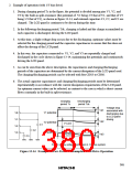
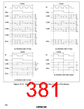
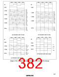
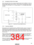
2. Example of operation (with 1/3 bias drive)
1. During charging period Tc in the figure, the potential is divided among pins V1, V2, and
V3 by the built-in split-resistance (the potential of V2 being 2/3 that of V1, and that of V3
being 1/3 that of V1), as shown in figure 13-14, and external capacitors C1, C2, and C3 are
charged. The LCD panel is continues to be driven during this time.
2. In the following discharging period, Tdc, charging is halted and the charge accumulated in
each capacitor is discharged, driving the LCD panel.
3. At this time, a slight voltage drop occurs due to the discharging; optimum values must be
selected for the charging period and the capacitor capacitances to ensure that this does not
affect the driving of the LCD panel.
4. In this way, the capacitors connected to V1, V2, and V3 are repeatedly charged and
discharged in the cycle shown in figure 13-14, maintaining the potentials and continuously
driving the LCD panel.
5. As can be seen from the above description, the capacitances and charging/discharging
periods of the capacitors are determined by the current dissipation of the LCD panel used.
The charging/discharging periods can be selected with bits CDS3 to CDS0.
6. The actual capacitor capacitances and charging/discharging periods must be determined
experimentally in accordance with the current dissipation requirements of the LCD panel.
An optimum current value can be selected, in contrast to the case in which a direct current
flows constantly in the built-in split-resistance.
Charging
period Tc
Discharging
period Tdc
Voltage drop
associated with
discharging due
to LCD panel
driving
Vd1
Vd2
V1 potential
V2 potential
V0
V1
V2
V3
V1×2/3
V1×1/3
C1
C2
V3 potential
Vd3
C3
Power supply voltage fluctuation in 1/3 bias system
Figure 13-14 Example of Low-Power-Consumption LCD Drive Operation
365

 ETC [ ETC ]