13.3.3
Luminance Adjustment Function (V0 Pin)
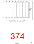
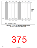
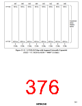
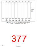
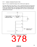
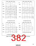
Figure 13-13 shows a detailed block diagram of the LCD drive power supply unit.
The voltage output to the V0 pin is either VCC or the 5 V output from the step-up conversion power
supply circuit. When either of these voltages is used directly as the LCD drive power supply, the
V0 and V1 pins should be shorted. Also, connecting a variable resistance, R, between the V0 and
V1 pins makes it possible to adjust the voltage applied to the V1 pin, and so to provide luminance
adjustment for the LCD panel.
VCC
V0
5V
Step-up constant-
voltage power supply
Power supply
selector
R
V1
V2
V3
Note: * Applied only to the
H8/3887 Series.
VSS
Figure 13-13 LCD Drive Power Supply Unit
363

 ETC [ ETC ]