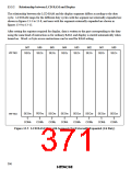
13.2.4
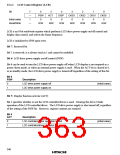
Clock Stop Register 2 (CKSTPR2)
Bit
7
—
1
6
—
1
5
—
1
4
—
1
3
2
1
0
AECKSTP WDCKSTP PWCKSTP LDCKSTP
Initial value
Read/Write
1
1
1
1
—
—
—
—
R/W
R/W
R/W
R/W
CKSTPR2 is an 8-bit read/write register that performs module standby mode control for peripheral
modules. Only the bit relating to the LCD controller/driver is described here. For details of the
other bits, see the sections on the relevant modules.
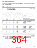
Bit 0: LCD controller/driver module standby mode control (LDCKSTP)
Bit 0 controls setting and clearing of module standby mode for the LCD controller/driver.
Bit 0
LDCKSTP
Description
0
1
LCD controller/driver is set to module standby mode
LCD controller/driver module standby mode is cleared
(initial value)
352

 ETC [ ETC ]