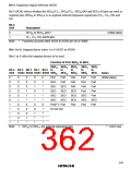
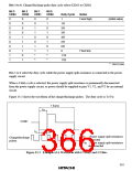
Bits 3 to 0: Charge/discharge pulse duty cycle select (CDS3 to CDS0)
Bit 3
Bit 2
Bit 1
Bit 0
CDS3
CDS2
CDS1
CDS0
Duty Cycle
Notes
0
0
0
0
0
0
0
0
1
1
0
0
0
0
1
1
1
1
0
1
0
0
1
1
0
0
1
1
*
*
0
1
0
1
0
1
0
1
*
*
1
Fixed high
(initial value)
1/8
2/8
3/8
4/8
5/8
6/8
0
Fixed low
1/16
1/32
*: Don’t care
Bits 3 to 0 select the duty cycle while the power supply split-resistance is connected to the power
supply circuit.
When a 0 duty cycle is selected, the power supply split-resistance is permanently disconnected
from the power supply circuit, so power should be supplied to pins V1, V2, and V3 by an external
circuit.
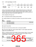
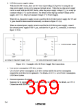
Figure 13-2 shows the waveform of the charge/discharge pulses. The duty cycle is Tc/Tw.
1 frame
T
W
COM1
Tc
Tdc
Tc : Power supply split-resistance
connected
Tdc : Power supply split-resistance
disconnected
Charge/discharge
pulses
Figure 13-2 Example of A Waveform with 1/2 Duty and 1/2 Bias
351

 ETC [ ETC ]